CD-700, VCXO Based PLL
12
9
11
10
13
CLAFGAB
FREQUENCY
VI YWW
14
15
16
8
7
6
5
1 2 3 4
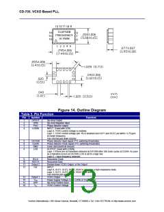
Figure 14. Outline Diagram
Table 5. Pin Function
Pin
1
Symbol
OPOUT
OPN
Function
Op-Amp Output
Op-Amp Negative Input
2
3
PHO
Phase detector output
4
LOSIN
INPUT (Used with LOS)
Logic 0, VCXO control voltage is enabled.
Logic 1, VCXO control voltage (pin 16) is disabled and OUT1 and OUT2 are within +/-75 ppm
of center frequency
Has Internal pull-down resistor
5
6
7
8
DATAIN
CLKIN
GND
Phase detector Input signal (TTL switching thresholds)
Phase detector Clock signal (TTL switching thresholds)
Cover and Electrical Ground
LOS
OUTPUT (Used with LOSIN)
Logic 1 if there are no transitions detected at DATAIN after 256 clock cycles at CLKIN. As soon
as a transition occurs at DATAIN, LOS is set to a logic low.
Logic 0 = Input frequency detected
9
RCLK
RDATA
Output 2
HIZ
Recovered Clock
Recovered Data
Divided-down VCXO Output, or No Output
INPUT
10
11
12
Logic 0, OUT1, OUT2, RCLK, RDATA are set to a high impedance state.
Logic 1, OUT1, OUT2, RCLK, RDATA are active.
Has Internal pull-up resistor
13
14
15
16
Output 1
VDD
OPP
VC
VCXO Output
Power Supply Voltage (3.3 V ±10% or 5.0 V ±10%)
Op-Amp Positive Input
VCXO Control Voltage
Vectron International • 166 Glover Avenue, Norwalk, CT 06856 • Tel: 1-88-VECTRON-1• http://www.vectron.com

 ETC [ ETC ]