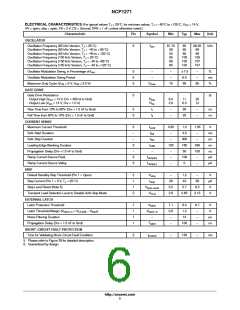
NCP1271
ELECTRICAL CHARACTERISTICS (For typical values T = 25°C, for min/max values, T = −40°C to +125°C, V = 14 V,
J
J
CC
HV = open, skip = open, FB = 2 V, CS = Ground, DRV = 1 nF, unless otherwise noted.)
Characteristic
Pin
Symbol
Min
Typ
Max
Unit
OSCILLATOR
Oscillation Frequency (65 kHz Version, T = 25_C)
5
f
61.75
58
55
95
89
65
65
65
100
100
100
68.25
69
69
105
107
107
kHz
J
osc
Oscillation Frequency (65 kHz Version, T = −40 to + 85_C)
J
Oscillation Frequency (65 kHz Version, T = −40 to + 125_C)
J
Oscillation Frequency (100 kHz Version, T = 25_C)
J
Oscillation Frequency (100 kHz Version, T = −40 to +85_C)
J
Oscillation Frequency (100 kHz Version, T = −40 to +125_C)
85
J
Oscillator Modulation Swing, in Percentage of f
5
5
5
−
−
−
−
"7.5
6.0
−
−
%
ms
%
osc
Oscillator Modulation Swing Period
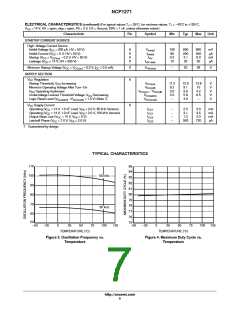
Maximum Duty Cycle (V = 0 V, V = 2.0 V)
D
max
75
80
85
CS
FB
GATE DRIVE
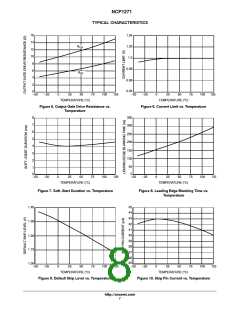
Gate Drive Resistance
5
W
Output High (V = 14 V, Drv = 300 W to Gnd)
R
R
6.0
2.0
11
6.0
20
12
CC
OH
Output Low (V = 14 V, Drv = 1.0 V)
CC
OL
Rise Time from 10% to 90% (Drv = 1.0 nF to Gnd)
Fall Time from 90% to 10% (Drv = 1.0 nF to Gnd)
5
5
t
−
−
30
20
−
−
ns
ns
r
t
f
CURRENT SENSE
Maximum Current Threshold
3
−
−
3
−
3
3
I
0.95
−
1.0
4.0
300
180
50
1.05
−
V
Limit
Soft−Start Duration
t
t
ms
ms
ns
ns
mA
mA
SS
Soft−Skip Duration
−
−
SK
Leading Edge Blanking Duration
Propagation Delay (Drv =1.0 nF to Gnd)
Ramp Current Source Peak
Ramp Current Source Valley
t
100
−
330
150
−
LEB
−
I
−
100
0
ramp(H)
I
−
−
ramp(L)
SKIP
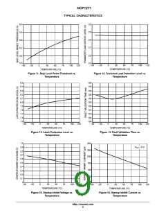
Default Standby Skip Threshold (Pin 1 = Open)
2
1
1
2
V
I
−
1.2
43
−
V
mA
V
skip
Skip Current (Pin 1 = 0 V, T = 25_C)
26
56
J
skip
Skip Level Reset (Note 5)
V
5.0
2.6
5.7
2.85
6.5
3.15
skip−reset
Transient Load Detection Level to Disable Soft−Skip Mode
V
TLD
V
EXTERNAL LATCH
Latch Protection Threshold
1
1
1
1
V
7.1
0.6
−
8.0
1.2
13
8.7
−
V
V
latch
Latch Threshold Margin (V
= V
− V
)
V
latch−m
latch−m
CC(off)
latch
Noise Filtering Duration
−
−
ms
ns
Propagation Delay (Drv = 1.0 nF to Gnd)
T
latch
−
100
−
SHORT−CIRCUIT FAULT PROTECTION
Time for Validating Short−Circuit Fault Condition
2
t
−
130
−
ms
protect
5. Please refer to Figure 39 for detailed description.
6. Guaranteed by design.
http://onsemi.com
5

 ETC [ ETC ]