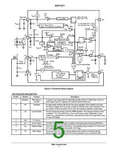
NCP1271
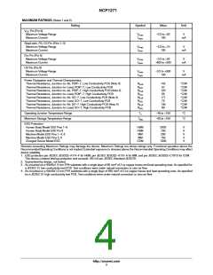
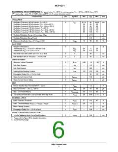
MAXIMUM RATINGS (Notes 1 and 2)
Rating
Symbol
Value
Unit
V
CC
Pin (Pin 6)
Maximum Voltage Range
Maximum Current
V
I
−0.3 to +20
V
mA
max
max
100
Skip/Latch, FB, CS Pin (Pins 1−3)
Maximum Voltage Range
Maximum Current
V
I
−0.3 to +10
V
mA
max
max
100
Drv Pin (Pin 5)
Maximum Voltage Range
Maximum Current
V
I
−0.3 to +20
−800 to +500
V
mA
max
max
HV Pin (Pin 8)
Maximum Voltage Range
Maximum Current
V
I
−0.3 to +500
V
mA
max
max
100
Power Dissipation and Thermal Characteristics
Thermal Resistance, Junction−to−Air, PDIP−7, Low Conductivity PCB (Note 3)
Thermal Resistance, Junction−to−Lead, PDIP−7, Low Conductivity PCB
Thermal Resistance, Junction−to−Air, PDIP−7, High Conductivity PCB (Note 4)
Thermal Resistance, Junction−to−Lead, PDIP−7, High Conductivity PCB
Thermal Resistance, Junction−to−Air, SO−7, Low Conductivity PCB (Note 3)
Thermal Resistance, Junction−to−Lead, SO−7, Low Conductivity PCB
Thermal Resistance, Junction−to−Air, SO−7, High Conductivity PCB (Note 4)
Thermal Resistance, Junction−to−Lead, SO−7, High Conductivity PCB
R
142
57
120
56
177
75
136
69
°C/W
°C/W
°C/W
°C/W
°C/W
°C/W
°C/W
°C/W
q
JA
R
R
q
JL
q
JA
R
R
q
JL
q
JA
R
q
JL
R
q
JA
R
q
JL
Operating Junction Temperature Range
Maximum Storage Temperature Range
T
−40 to +150
−60 to +150
°C
°C
J
T
stg
ESD Protection
Human Body Model ESD Pins 1−6
Human Body Model ESD Pin 8
Machine Model ESD Pins 1−4, 8
Machine Model ESD Pins 5, 6
Charged Device Model ESD
HBM
HBM
MM
MM
CDM
2000
700
200
150
1000
V
V
V
V
V
Stresses exceeding Maximum Ratings may damage the device. Maximum Ratings are stress ratings only. Functional operation above the
RecommendedOperating Conditions is not implied. Extended exposure to stresses above the Recommended Operating Conditions may affect
device reliability.
1. ESD protection per JEDEC JESD22−A114−F for HBM, per JEDEC JESD22−A115−A for MM, and per JEDEC JESD22−C101D for CDM.
This device contains latchup protection and exceeds 100 mA per JEDEC Standard JESD78.
2. Guaranteed by design, not tested.
2
3. As mounted on a 40x40x1.5 mm FR4 substrate with a single layer of 80 mm of 2 oz copper traces and heat spreading area. As specified for
a JEDEC 51 low conductivity test PCB. Test conditions were under natural convection or zero air flow.
2
4. As mounted on a 40x40x1.5 mm FR4 substrate with a single layer of 650 mm of 2 oz copper traces and heat spreading area. As specified
for a JEDEC 51 high conductivity test PCB. Test conditions were under natural convection or zero air flow.
http://onsemi.com
3

 ETC [ ETC ]