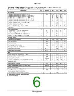
NCP1271
8 V
I
skip
latch−off, reset
when Vcc < 4V
Skip/ latch
−
+
13 us filter
S
R
1
8
HV
Q
4.1 mA when Vcc > 0.6 V
0.2 mA when Vcc < 0.6 V
R
10V
skip
V
V
skip
V
V
= R
* I
or
skip
skip
skip skip
= 1.2 V when pin 1 is opened
skip
+
−
turn off
FB
4.8 V
16.7k
2.85 V
12.6/
5.8 V
disable
soft
TLD
V
soft−skip
FB
FB
−
+
skip
2
−
+
S
V
ss
Soft start/ soft−skip
management
4 ms/ 300 us
75.3k
(1V max)
Q
R
UVLO
soft
start
1 / 3
/ 3
−
+
double
hiccup
B2
130ms
10V
V
V
FB
delay
&
0
1
9.1 V
short
circuit
fault
Counter
V
CC
PWM
−
+
−
V
PWM
CS
6
+
CS
180 ns
LEB
3
&
20V
10V
100uA
0
R
ramp
turn on internal bias
V
OR
jittered ramp
current source
CC
R
CS
Drv
4
Gnd
5
R
S
Q
7.5% Jittering
65, 100 kHz
Oscillator
1
0
driver:
+500 mA
/ −800 mA
Max duty
= 80%
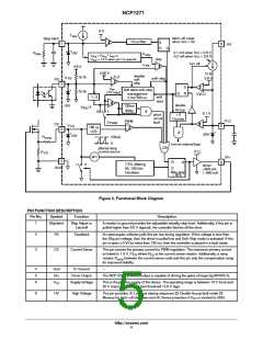
Figure 2. Functional Block Diagram
PIN FUNCTION DESCRIPTION
Pin No.
Symbol
Function
Description
1
Skip/latch
Skip Adjust or
Latchoff
A resistor to ground provides the adjustable standby skip level. Additionally, if this pin is
pulled higher than 8.0 V (typical), the controller latches off the drive.
2
3
FB
CS
Feedback
An optocoupler collector pulls this pin low during regulation. If this voltage is less than
the Skip pin voltage, then the driver is pulled low and Soft−Skip mode is activated. If this
pin is open (>3 V) for more than 130 ms, then the controller is placed in a fault mode.
Current Sense
This pin senses the primary current for PWM regulation. The maximum primary current
is limited to 1.0 V / R where R is the current sense resistor. Additionally, a ramp
CS
CS
resistor R
between the current sense node and this pin sets the compensation ramp
ramp
for improved stability.
4
5
6
Gnd
Drv
IC Ground
Driver Output
Supply Voltage
−
The NCP1271’s powerful output is capable of driving the gates of large Qg MOSFETs.
V
CC
This is the positive supply of the device. The operating range is between 10 V (min) and
20 V (max) with a UVLO start threshold 12.6 V (typ).
8
HV
High Voltage
This pin provides (1) Lossless startup sequence (2) Double hiccup fault mode (3)
Memory for latch−off shutdown and (4) Device protection if V is shorted to GND.
CC
http://onsemi.com
4

 ETC [ ETC ]