LH52256C/CH
CMOS 256K (32K × 8) Static RAM
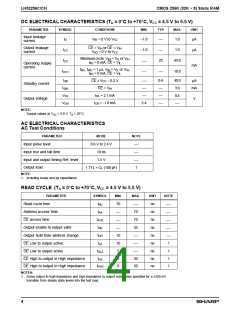
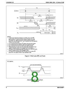
tWC
ADDRESS
tAW
tWR
tCW
(NOTE 4)
(NOTE 2
)
CE
tWR
tAS
tWP
(NOTE 4)
(NOTE 1)
(NOTE 3)
WE
tWZ
tOW
(NOTE 6)
(NOTE 7)
DOUT
tDW
tDH
(NOTE 5)
DIN
DATA VALID
NOTES:
1. A write occurs during the overlap of a LOW CE, and a LOW WE.
A write begins at the latest transition among CE going LOW, and
WE going LOW. A write ends at the earliest transition among CE
going HIGH, and WE going HIGH. tWP is measured from the beginning
of write to the end of write.
2. tCW is measured from the later of CE going LOW to the end of write.
3. tAS is measured from the address valid to the beginning of write.
4. tWR is measured from the end of write to the address change.
5. During this period, I/O pins are in the output state, therefore the input
signals of opposite phase to the outputs must not be applied.
6. If CE goes LOW simultaneously with WE going LOW or after WE going
LOW, the outputs remain in high impedance state.
7. If CE goes HIGH simulaneously with WE going HIGH or before WE
going HIGH, the outputs remain in high impedance state.
52256C-5
Figure 6. Write Cycle (OE Low Fixed)
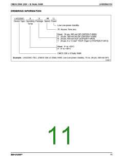
CE CONTROL
DATA RETENTION MODE
VCC
4.5 V
tCDR
tR
2.2 V
VCCDR
CE ≥ VCCDR - 0.2 V
CE
0 V
52256C-6
Data Retention Timing Chart
CE Controlled
8

 ETC [ ETC ]