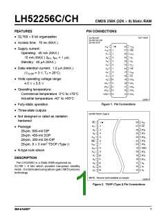
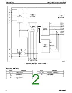
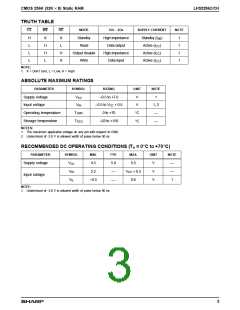
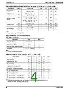
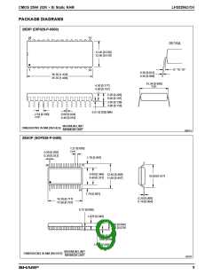
CMOS 256K (32K × 8) Static RAM
LH52256C/CH
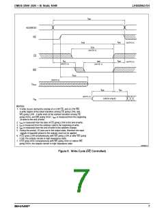
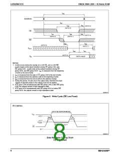
WRITE CYCLE (TA = 0°C to +70°C, VCC = 4.5 V to 5.5 V)
PARAMETER
SYMBOL
MIN.
70
45
45
0
MAX.
UNIT
ns
ns
ns
ns
ns
ns
ns
ns
ns
NOTE
Write cycle time
tWC
CE Low to end of write
Address valid to end of write
Address setup time
tCW
tAW
tAS
Write pulse width
tWP
35
0
Write recovery time
tWR
Input data setup time
Input data hold time
WE High to output active
tDW
30
0
tDH
tOW
5
1
1
WE Low to output in High
impedance
tWZ
0
0
30
30
ns
ns
OE High to output in High
impedance
tOHZ
1
NOTE:
1.
Active output to high-impedance and high-impedance to output active tests specified for a ±200 mV
transition from steady state levels into the test load.
CAPACITANCE (TA = 25°C, f = 1MHz)
PARAMETER
Input capacitance
I/O capacitance
SYMBOL
CONDITIONS
MIN.
TYP.
MAX.
7
UNIT
pF
NOTE
CIN
VIN = 0 V
1
1
CI/O
VI/O = 0 V
10
pF
NOTE:
1. This parameter is sampled and not production tested.
DATA RETENTION CHARACTERISTICS (TA = 0°C to +70°C)
PARAMETER
SYMBOL
CONDITIONS
MIN.
TYP.
MAX.
5.5
UNIT
NOTE
Data retention supply voltage
VCCDR
CE ≥ VCCDR – 0.2 V
2.0
V
VCCDR = 3.0 V
0.3
1.0
TA = 25°C
TA = 40°C
Data retention supply current
ICCDR
µA
3.0
CE ≥ VCCDR – 0.2 V
15
Chip enable setup time
Chip enable hold time
tCDR
tR
0
ns
ns
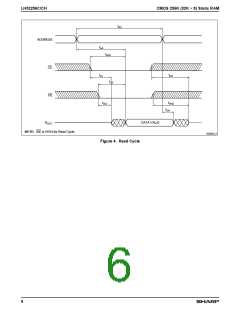
tRC
1
NOTE:
1. tRC = Read cycle time.
2.
Typical values at TA = 25°C
5

 ETC [ ETC ]