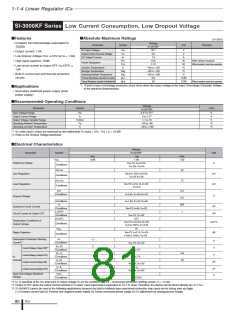
1-1-4 Linear Regulator ICs
SI-3000KWM Series 2-Output, Surface-Mount, Low Dropout Voltage
■Features
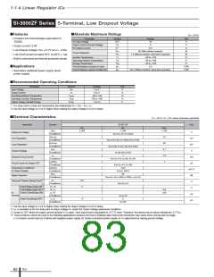
■Absolute Maximum Ratings
(Ta=25°C)
• Compact surface-mount package (TO252-5)
Ratings
Parameter
Symbol
Unit
SI-3002KWM
• Output current: 1.0A × 2
*1
DC Input Voltage
VIN
18
V
V
• Low dropout voltage: VDIF ≤ 0.6V (at IO = 1A)
Output Control Terminal Voltage
Output Current*1
VC
IO1
IO2
6
• Built-in overcurrent and thermal protection
circuits
1.0
A
1.0
*2
Power Dissipation (with two outputs ON)
Junction Temperature
PD
1
W
°C
Tj
–30 to +125
–30 to +85
–40 to +125
95
■Applications
• Secondary stabilized power supply (local
power supply)
Operating Ambient Temperature
Storage Temperature
Top
Tstg
θj-a
θj-c
°C
°C
Thermal Resistance (Junction to Ambient Air)
Thermal Resistance (Junction to Lead)
°C/W
°C/W
6
*1: VIN (max), IO1 (max) and IO2 (max) are restricted by the relation PD = (VIN – VO1) × IO1 + (VIN - VO2) × IO2.
*2: When mounted on glass-epoxy board of 30 × 30mm2 (copper laminate area 4.3%)
Thermal protection may operate when the junction temperature exceeds 135°C.
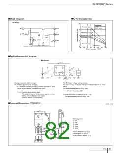
■Electrical Characteristics
Ratings
Parameter
Symbol
SI-3002KWM
Unit
V
min.
typ.
3.300
max.
VO1
3.234
3.366
Conditions
VO2
VIN=5V, IO=10mA
2.500
Output Voltage
2.450
2.550
20
Conditions
∆VOLINE1
Conditions
∆VOLINE2
Conditions
∆VOLOAD1
Conditions
∆VOLOAD2
Conditions
VDIF1
VIN=5V, IO=10mA
VIN=4.5 to 10V, IO=10mA
VIN=4.5 to 10V, IO=10mA
VIN=5V, IO=0 to 1A
mV
Line Regulation
20
30
mV
V
Load Regulation
Dropout Voltage
30
VIN=5V, IO=0 to 1A
0.6
Conditions
∆VO1/∆Ta
Conditions
∆VO2/∆Ta
Conditions
RREJ1
IO=1A
±0.3
Temperature Coefficient of
Output Voltage
Tj=0 to 100°C
mV/°C
±0.3
Tj=0 to 100°C
60
Conditions
RREJ2
VIN=5V, f=100 to 120Hz
60
dB
A
Ripple Rejection
Conditions
IS1 1
VIN=5V, f=100 to 120Hz
1.2
1.2
Overcurrent Protection Starting
Current*1
Conditions
IS1 2
VIN=5V
Conditions
Iq
VIN=5V
1
1.5
0.5
mA
mA
Quiescent Circuit Current
Conditions
Iq (OFF)
VIN=5V, IO=0A, VC=2V
Circuit Current at Output OFF
Control Voltage (Output ON)
Conditions
VC, IH
VIN=5V, VC=0V
*2
2
V
V
Control Voltage (Output OFF)
VC, IL
0.8
5
VC
Control Current
(Output ON)
IC, IH
µA
Terminal
Conditions
IC, IL
VC=2.7V
VC=0.4V
Control Current
(Output OFF)
–100
µA
Conditions
VO(OFF)
Output OFF Voltage
0.5
V
*1: IS1 1 and IS1 2 are specified at the 5% drop points of output voltages VO1 and VO2 on the condition that VIN = the condition of protection starting current, IO = 10 mA.
*2: Output is ON when the output control terminal VC is open. Each input level is equivalent to LS-TTL. Therefore, the devices can be driven directly by LS-TTLs.
Channels 1 and 2 are turned on or off at the same time.
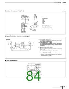
ICs
84

 ETC [ ETC ]