NR885K
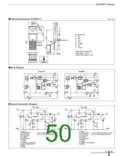
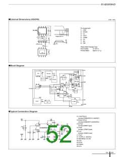
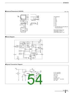
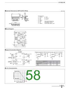
■External Dimensions (HSOP8)
(Unit : mm)
Pin 1
Mark
Pin Assignment
q
w
e
r
t
y
u
i
BS
VIN
SW
GND
FB
Enlarged View of A
0.695 TYP
5.20
A
NC
EN
SS
0.4
1.27
0.40
*: The heat slug on the rear side is at
the ground potential.
Plastic Mold Package Type
Flammability: UL 94V-0
2.90
Product Mass: Approx. 0.1g
■Block Diagram
2
IN
Σ
Current
Sense
OSC
BS
Drive
REG
1
3
3.5V
0.8V
OCP
ON/
OFF
P.REG
VREF
7
5V
EN
SW
+
-
PWM
LOGIC
5V
TSD
Compensation
UVLO
FB
5
-
+
6
NC
+
0.8V
3.5V
Error Amp
10uA
SS
SS
GND
4
8
■Typical Connection Diagram
VIN
R3
C10
2
1
Vout
L1
VIN
EN
BS
3
5
7
SW
FB
C1, C2: 10µF/25V
C4, C5: 22µF/16V
C9: 0.1µF
C2
C1
NR885K
R4
R5
C4 C5
8
SS
GND
4
NC
6
C10: 0.1µF
C9
L1: 10µH
R6
R3: 20Ωto 47Ω
R4+R5: 5kΩꢀꢀ(VO=3.3V)
R6: 1.6kΩ
D1
ICs
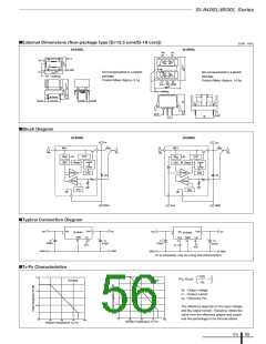
53

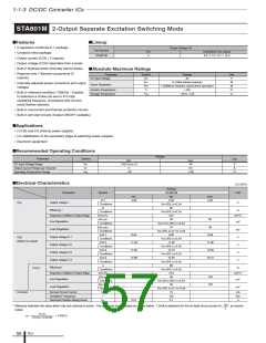
 ETC [ ETC ]