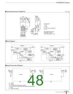
1-1-3 DC/DC Converter ICs
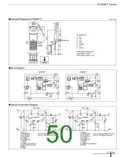
SI-8205NHD
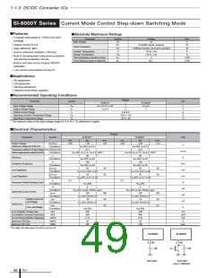
FSuurlfl-aMceo-Mldo,uSnepCaurarrteentEMxcoidteatCioonntSrotle, pS-ydnochwronnSouwsitRcehcintigfieMr Sotdeep-RdoewgnulSawtoitrchICinsg Mode
t,
■Features
■Absolute Maximum Ratings
Parameter
Symbol
VIN
PD
Ratings
46
Unit
V
Conditions
• Compact surface-mount (HSOP8) package
Input Voltage (VIN Pin)
Power Dissipation
• Wide input voltage range (VIN): Vo + 3 to 43 V
• Synchronous rectifier mode
1.35
W
When mounted on a 30 × 30 mm glass-epoxy board (with a 25 × 25 mm copper area)
When mounted on a 30 × 30 mm glass-epoxy board (with a 25 × 25 mm copper area)
Junction Temperature
Tj
–40 to +150
°C
°C
• Output current: 3 A
Storage Temperature
Tstg
θj-c
–40 to +150
Thermal Resistance (Junction to Lead <1 pin>)
Thermal Resistance (Junction to Ambient Air)
40
74
°C/W
°C/W
• Reference voltage and accuracy of 0.5 V ±1%
• Oscillation frequency: 200 kHz to 1 MHz
• A ceramic capacitor can be used for output
• Output can be disabled
θj-a
■Recommended Operating Conditions
Parameter
Symbol
Ratings
Unit
V
• Undervoltage Lock Out
Input Voltage Range
VIN
8 or Vo+3 to 43
0 to 3.0
• Soft start function
Output Current Range
Io
A
Output Voltage Range
Vo
0.5 to 24
V
■Applications
Operating Junction Temperature Range
Operating Temperature Range
Tjop
Top
–40 to +125
–40 to +85
°C
°C
• Power supply for LCD module
• Power supply for notebook PC
• Onboard local power supplies
• Power supply for LBP/PPC
*: The minimum value of the input voltage range is 8 V or Vo + 3V, whichever is higher.
■Electrical Characteristics
(Ta = 25°C and fo = 500kHz, unless otherwise specified)
Ratings
typ.
0.500
±0.05
90
Parameter
Symbol
Unit
Conditions
min.
max.
Reference Voltage
Vref
∆VREF/∆T
η
0.495
0.505
V
mV/°C
%
VIN=12V, Io=1.0A
Temperature Coefficient of Reference Voltage
Efficiency
VIN=12V, Io=1.0A, Ta=–40 to +85°C
VIN=12V, Vo=5V, Io=1.0A
VIN=12V, Vo=5V, Io=1A, Rfset=375kΩ
VIN=12V, Vo=5V, Io=1A, Rfset=75kΩ
VIN=8 to 43V, Vo to 5V, Io=1A
VIN=12V, Vo=5V, Io=0.1 to 3.0A
VIN=12V, Vo=5V
Oscillation Frequency 1
Oscillation Frequency 2
Line Regulation
fo1
200
1
kHz
MHz
mV
mV
A
fo2
∆VoLINE
∆VoLOAD
Is
50
Load Regulation
50
Overcurrent Protection Starting Current
3.1
6.0
40
IIN
8
mA
µA
VIN=12V, Vcomp=0V
Quiescent Circuit Current
IIN(OFF)
IEN/SS
VSSH
VC/EH
Vovp
VIN=12V, VEN/ss=0V
Outflow Current at Low Voltage
5
µA
VEN/SS=0V, VIN=12V
EN/SS Pin
Open Voltage
3.0
0.6
4.5
6.0
2.0
V
VIN=12V
On Threshold Voltage
1.3
V
VIN=12V
OVP Start Voltage
0.57
151
0.60
160
800
800
3.33
90
0.63
V
Thermal Protection Start Temperature
Error Amplifier Voltage Gain
Error Amplifier Transformer Conductance
Current Sense Amplifier Impedance
Maximum ON Duty
Tj
°C
AEA
GEA
GCS
DMAX
DMIN
V/V
µA/V
A/V
%
80
VIN=12V
VIN=12V
Minimum ON Time
150
nsec
ICs
50

 ETC [ ETC ]