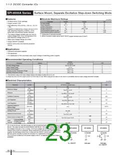
1-1-3 DC/DC Converter ICs
SI-8000TM Series Surface-Mount, Separate Excitation Step-down Switching Mode
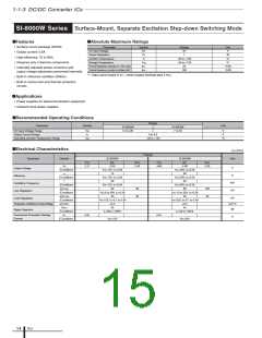
■Features
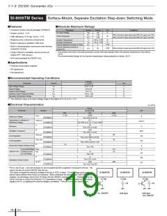
■Absolute Maximum Ratings
• Compact surface-mount package (TO252-5)
Parameter
Symbol
Ratings
43
Unit
V
Conditions
DC Input Voltage
VIN
• Output current: 1.5 A
PD1
PD2
Tj
1.06
When mounted on glass-epoxy board (900 mm2 copper area 4.3%)
When mounted on glass-epoxy board (900 mm2 copper area 50%)
Power Dissipation
W
• High efficiency: 81% typ. (at Vo = 5 V)
• Requires only 4 discrete components
• Built-in reference oscillator (300 kHz)
1.65
Junction Temperature*
–30 to +150
–40 to +150
6
°C
°C
Storage Temperature
Tstg
θj-c
Thermal Resistance (Junction to Case)
°C/W
• Built-in drooping-type-overcurrent and thermal
protection circuits
Thermal Resistance (Junction to
Ambient Air)
θj-a
95
°C/W
When mounted on glass-epoxy board (900 mm2 copper area 4.3%)
*: This product has built-in thermal protection circuits that may operate when the junction temperature rises above
130°C.
The recommended design for the junction temperature during operation is below 125°C.
• Output ON/OFF available (circuit current at
output OFF: 200 µA typ.)
• Soft start available by ON/OFF pin
■Applications
• Onboard local power supplies
• AV equipment
• OA equipment
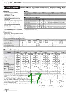
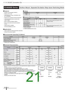
■Recommended Operating Conditions
Ratings
Parameter
Symbol
Unit
SI-8008TM
Input Voltage Range
VIN
VO
IO
V
O
+3*1 to 40
V
V
Output Voltage
0.8 to 24
0 to 1.5
Output Current Range
A
Operating Junction Temperature Range
Operating Temperature Range
Tjop
Top
–20 to +100
–20 to +85
°C
°C
*1: The minimum value of an input voltage range is the higher of 4.5 V or VO + 3 V.
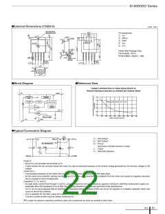
■Electrical Characteristics
(Ta=25°C)
Rating
SI-8008TM
typ.
Parameter
Symbol
Unit
min.
max.
0.784
0.800
0.816
V
ADJ
V
mV/°C
%
Reference Voltage
Conditions
V
IN=15V, I
o=0.1A
0.1
Temperature Coefficient of
Reference Voltage
∆VADJ/∆
T
Conditions
Conditions
Conditions
Conditions
Conditions
Conditions
V
IN=15V, I
o
=0.1A, T
81
c=0 to 100°C
η
Efficiency
V
V
IN=15V, I
o
=0.5A
=0.5A
fo
300
Oscillation Frequency
Line Regulation
Load Regulation
kHz
mV
IN=15V, I
60
o
80
40
∆VOLINE
V
V
IN=10 to 30V, I
10
o=0.5A
∆VOLOAD
mV
IN=15V, Io=0.2 to 1.5A
I
S
1.6
Overcurrent Protection Starting Current
Low Level Voltage
A
V
V
IN=15V
V
SSL
0.5
40
ON/OFF Pin*
Outflow Current
at Low Voltage
I
I
I
SSL
10
µ
A
V
SSL=0V
6
Conditions
Conditions
Conditions
q
mA
V
IN=15V, I
200
o=0A
Quiescent Circuit Current
q (OFF)
400
µ
A
V
IN=15V, VSS=0V
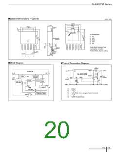
*: Pin 5 is the SS pin. Soft start at power on can be performed with a capacitor connected to this pin. The
output can also be turned ON/OFF with this pin.
The output is stopped by setting the voltage of this pin to VSSL or lower. SS-pin voltage can be changed
with an open-collector drive circuit of a transistor. When using both the soft-start and ON/OFF functions
together, the discharge current from C3 flows into the ON/OFF control transistor. Therefore, limit the
current securely to protect the transistor if C3 capacitance is large. The SS pin is pulled up to the power
supply in the IC, so applying the external voltage is prohibited. If the pin is not used, leave it open.
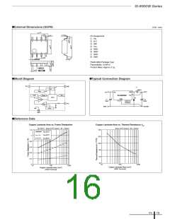
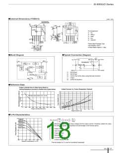
SI-8000TM
SI-8000TM
SI-8000TM
5
SS
5
SS
C3
5 SS
C3
VO. ON/OFF
Soft start
Soft start
+VO. ON/OFF
ICs
18

 ETC [ ETC ]