6
Notes:
6. Beyond the full-scale input range the
output is either all zeroes or all ones.
7. The effective number of bits (or
effective resolution) is defined by the
equation ENOB = (SNR-1.76)/6.02
and represents the resolution of an
ideal, quantization-noise limited A/D
converter with the same SNR.
8. Conversion time is defined as the
time from when the convert start
signal CS is brought low to when
SDAT goes high, indicating that
output data is ready to be clocked
out. This can be as small as a few
cycles of the isolated modulator clock
and is determined by the frequency of
the isolated modulator clock and the
selected Conversion and Pre-Trigger
modes. For determining the true
signal delay characteristics of the A/D
converter for closed-loop phase
determining the true signal delay
characteristics of the A/D converter
and should be used for determining
phase margins in closed-loop applica-
tions. The signal delay is determined
by the frequency of the modulator
clock and which Conversion Mode is
selected, and is independent of the
selected Pre-Trigger Mode and,
therefore, conversion time.
1. Resolution is defined as the total
number of output bits. The useable
accuracy of any A/D converter is a
function of its linearity and signal-to-
noise ratio, rather than how many
total bits it has.
2. Integral nonlinearity is defined as
one-half the peak-to-peak deviation
of the best-fit line through the
transfer curve for VIN+ = -200 mV to
+200 mV, expressed either as the
number of LSBs or as a percent of
measured input range (400 mV).
3. Differential nonlinearity is defined as
the deviation of the actual difference
from the ideal difference between
midpoints of successive output
codes, expressed in LSBs.
4. Data sheet value is the average
magnitude of the difference in offset
voltage from TA = 25°C to TA = 85°C,
expressed in microvolts per °C.
Three standard deviation from typical
value is less than 6 µV/°C.
5. All units within each HCPL-7860
standard packaging increment (either
50 per tube or 1000 per reel) have an
Absolute Reference Voltage tolerance
of ± 1%. All units within each HCPL-
786J standard packaging increment
(either 50 per tube or 1000 per reel)
have an Absolute Reference Voltage
tolerance of ± 2%. An Absolute
Reference Voltage tolerance of ± 4%
is guaranteed between standard
packaging increments.
10. The minimum and maximum over-
range detection time is determined by
the frequency of the channel 1 iso-
lated modulator clock.
11. The minimum and maximum thresh-
old detection time is determined by
the user-defined configuration of the
adjustable threshold detection circuit
and the frequency of the channel 1
isolated modulator clock. See the
Applications Information section for
further detail. The specified times
apply for the default configuration.
12. The signal bandwidth is the
frequency at which the magnitude of
the output signal has decreased 3 dB
below its low-frequency value. The
signal bandwidth is determined by
the frequency of the modulator clock
and the selected Conversion Mode.
13. The isolation transient immunity
(also known as Common-Mode
Rejection) specifies the minimum
rate-of-rise of an isolation-mode
signal applied across the isolation
boundary beyond which the
margin calculations, the signal delay
specification should be used.
9. Signal delay is defined as the effec-
tive delay of the input signal through
the Isolated A/D converter. It can be
measured by applying a -200 mV to
± 200 mV step at the input of modu-
lator and adjusting the relative delay
of the convert start signal CS so that
the output of the converter is at mid-
scale. The signal delay is the elapsed
time from when the step signal is
applied at the input to when output
data is ready at the end of the conver-
sion cycle. The signal delay is the
most important specification for
modulator clock or data signals are
corrupted.
7
0.02
68
V
V
V
= 4.5 V
= 5.0 V
= 5.5 V
V
V
V
= 4.5 V
= 5.0 V
= 5.5 V
0.018
0.016
0.014
0.012
0.01
DD1
DD1
DD1
DD1
DD1
DD1
67
66
65
64
63
6
5
4
3
2
V
V
V
= 4.5 V
= 5.0 V
= 5.5 V
DD1
DD1
DD1
0.008
0.006
62
61
-40
-15
10
35
60
85
-40
-15
10
35
60
85
-40
-15
10
35
60
85
TEMPERATURE – °C
TEMPERATURE – °C
TEMPERATURE – °C
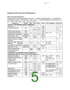
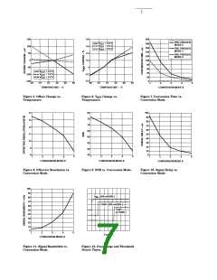
Figure 2. SNR vs. Temperature.
Figure 3. INL (Bits) vs. Temperature.
Figure 4. INL (%) vs. Temperature.

 ETC [ ETC ]