5
Isolated A/D Converter Performance
Electrical Specifications
Unless otherwise noted, all specifications are at V
= -200 mV to +200 mV and V = 0 V; all Typical
IN-
IN+
specifications are at T = 25°C and V
= V = V = 5 V; all Minimum/Maximum specifications are at
DD2 DD
A
DD1
T = -40°C to +85°C, V
= V = V = 4.5 to 5.5 V.
DD2 DD
A
DD1
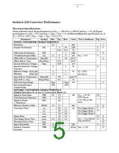
Parameter
Symbol
Min. Typ. Max. Units Test Conditions Fig. Note
STATIC CONVERTER CHARACTERISTICS
Resolution
15
bits
LSB
%
LSB
mV
µV/°C
mV/V
mV
1
2
Integral Nonlinearity
INL
3
30
3
4
0.01 0.14
1
Differential Nonlinearity
Uncalibrated Input Offset
Offset Drift vs. Temperature
DNL
3
4
V
-3
0
2
3
10
V
IN+
= 0 V
5
OS
dV /dT
OS
A
Offset drift vs. V
Internal Reference Voltage
dV /dV
DD1
0.12
320
DD1
OS
V
REF
Absolute Reference Voltage
Tolerance
-4
4
%
6
Reference Voltage HCPL-7860
-1
-2
1
2
%
T = 25°C.
See Note 5
A
Matching
HCPL-786J
V
Drift vs. Temperature dV
/dT
A
/dV
DD1
60
0.2
ppm/°C
%
REF
REF
V
REF
Drift vs. V
dV
DD1
REF
Full Scale Input Range
-V
REF
+V
mV
5
REF
Recommended Input
Voltage Range
-200
+200
DYNAMIC CONVERTER CHARACTERISTICS
(Digital Interface IC is set to Conversion Mode 3.)
Signal-to-Noise Ratio
Total Harmonic Distortion
Signal-to-(Noise
+ Distortion)
SNR
THD
SND
62
73
-67
66
dB
V
= 35 Hz,
2,9
8
IN+
400 mV
pk-pk
(141 mV ) sine
wave.
rms
Effective Number of Bits
Conversion Time
ENOB
10
12
0.8
20
40
20
3.0
10
22
20
bits
µs
6
7
t
t
t
1.1
24
48
24
4.2
Pre-Trigger Mode 2 7,
Pre-Trigger Mode 1
Pre-Trigger Mode 0
10
C2
C1
C0
14
Signal Delay
t
8
9
10
11
12
DSIG
Over-Range Detect Time
Threshold Detect Time
Signal Bandwidth
Isolation Transient
Immunity
t
t
2.0
V
= 0 to 400 mV 12
OVR1
IN+
step waveform
THR1
BW
CMR
18
15
kHz
kV/µs
11
V
ISO
= 1 kV

 ETC [ ETC ]