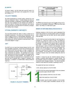
.) Choose the two bandwidths following the guidelines in the
General Setup Considerations; the RV resistor must be the same
value for both bandwidthsꢀ
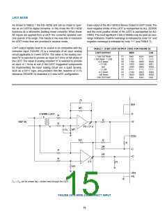
The Converter Busy (CB) signal indicates that the tracking con-
verter output angle is changing 1 LSBꢀ As shown in FIGURE .0,
output data is valid 50 nS maximum after the middle of the CB
pulseꢀ CB pulse width is 1/40 FS, which is nominally 375 nsꢀ
3) Use the SHIFT pin to choose between bandwidthsꢀ A logic 1
selects the VEL1 components and a logic 0 selects the VEL.
componentsꢀ
INTERNAL ENCODER EMULATION
The RD-19.30 can be programmed to encoder emulation mode
by connecting the A_QUAD_B input to GNDꢀ The U/B output pin
becomes B (LSB XOR LSB + 1) The A (LSB + 1) and B output
signals can be used in control systems that are designed to inter-
face with incremental optical encodersꢀ To enable the Zero Index
pulse, ZIP_EN should be tied to GNDꢀ
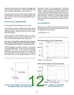
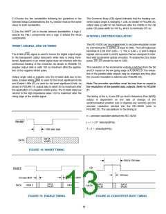
INHIBIT, ENABLE, AND CB TIMING
The Inhibit (INH) signal is used to freeze the digital output angle
in the transparent output data latch while data is being trans-
ferredꢀ Application of an Inhibit signal does not interfere with the
continuous tracking of the converterꢀ As shown in FIGURE 18,
angular output data is valid 150 ns maximum after the applica-
tion of the negative inhibit pulseꢀ
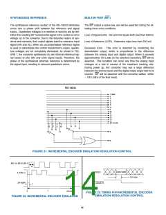
The resolution of the incremental outputs is latched from the D0
and D1 inputs on the low going edge of A_QUAD_BꢀThe resolu-
tion of the parallel data outputs may be changed any time after
the encoder resolution is latched (see FIGURE .3)ꢀ
Output angle data is enabled onto the tri-state data bus in two
bytesꢀ Enable MSBs (EM) is used for the most significant 8 bits
and Enable LSBs (EL) is used for the least significant 8 bitsꢀ As
shown in FIGURE 19, output data is valid 150 ns maximum after
the application of a negative enable pulseꢀ The tri-state data bus
returns to the high impedance state 100 ns maximum after the
rising edge of the enable signalꢀ
Note: The encoder resolution must be less than or equal to
the resolution of the parallel data outputs. Refer to FIGURE
21.
The timing of the A, B and ZIP (or North Reference Pole [NRP])
output is dependent on the rate of change of the
synchro/resolver position (rps or degrees per second) and the
encoder resolution latched into the RD-19.30 (refer to
FIGURE ..)ꢀ The calculations for the timing is:
n = encoder resolution latched into RD-19.30
t = 1 / ( .n* Velocity(RPS))
INHIBIT
T = 1 / ( Velocity(RPS))
150 nsec max
DATA
DATA
VALID
FIGURE 18. INHIBIT TIMING
.50 to 750 nsec
CB
ENABLE
50 nsec
100 nsec MAX
HIGH Z
150 nsec MAX
DATA
VALID
DATA
VALID
DATA
VALID
DATA
HIGH Z
DATA
FIGURE 19. ENABLE TIMING
FIGURE 20. CONVERTER BUSY TIMING
13

 ETC [ ETC ]