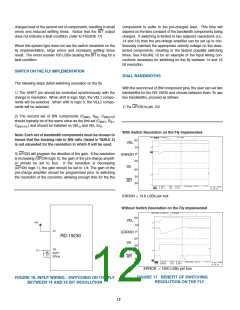
charged level of the second set of components, resulting in small
errors and reduced settling timesꢀ Notice that the BIT output
does not indicate a fault conditionꢀ (refer to FIGURE 17)
components to settle to the pre-charged levelꢀ This time will
depend on the time constant of the bandwidth components being
chargedꢀ If switching is limited to two adjacent resolutions (iꢀeꢀ,
14 and 16) then the pre-charge amplifier can be set up to con-
tinuously maintain the appropriate velocity voltage on the dese-
lected components, resulting in the fastest possible switching
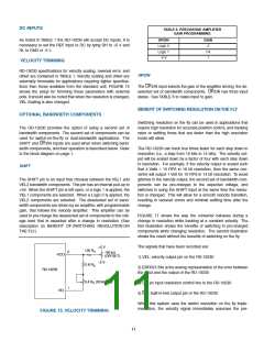
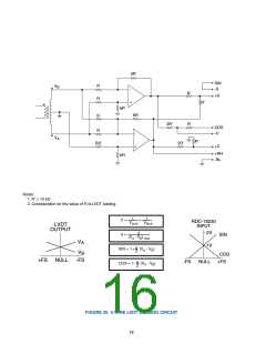
timesꢀ See FIGURE 16 for an example of the input wiring con-
nections necessary for switching on the fly between 14 and 16
bit resolutionꢀ
When this system type does not use the switch resolution on the
fly implementation, large errors and increased settling times
resultꢀ The errors exceed 100 LSBs causing the BIT to flag for a
fault conditionꢀ
SWITCH ONTHE FLY IMPLEMENTATION
DUAL BANDWIDTHS
The following steps detail switching resolution on the flyꢀ
With the second set of BW component pins, the user can set two
bandwidths for the RD-19.30 and choose between themꢀ To use
two bandwidths, proceed as follows:
1) The SHIFT pin should be controlled synchronously with the
change in resolutionꢀ When shift is logic high, the VEL1 compo-
nents will be selectedꢀ When shift is logic 0, the VEL. compo-
nents will be selectedꢀ
1) Tie UP/DN to pin -5Vꢀ
.) The second set of BW components (CBW., RB., CBW./10
should typically be of the same value as the first set (CBW1, RB1
BW1/10,) and should be installed on VEL. and VEL SJ.ꢀ
)
,
C
With Switch Resolution on the Fly Implemented
Note: Each set of bandwidth components must be chosen to
insure that the tracking rate to BW ratio (listed in TABLE 2)
is not exceeded for the resolution in which it will be used.
VEL 0V
-5V
3) UP/DN will program the direction of the gainꢀ If the resolution
is increasing (UP/DN logic 0), the gain of the pre-charge amplifi-
er should be set to fourꢀ If the resolution is decreasing
(UP/DN logic 1), the gain should be set to 1/4ꢀ The gain of the
pre-charge amplifier should be programmed prior to switching
the resolution of the converter, allowing enough time for the the
0°
ERROR
5V
D0
0V
5V
BIT
0V
ERROR = 13ꢀ6 LSBs per box
Without Switch Resolution on the Fly Implemented
VEL 0V
+5V
-5V
D1
0°
ERROR
RD-19.30
5V
D0
0V
D0
58
5V
SHIFT
.7
UP/DN
BIT
0V
ERROR = 1500 LSBs per box
FIGURE 17. BENEFIT OF SWITCHING
RESOLUTION ON THE FLY
FIGURE 16. INPUT WIRING - SWITCHING ON THE FLY
BETWEEN 14 AND 16 BIT RESOLUTION
12

 ETC [ ETC ]