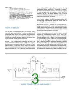
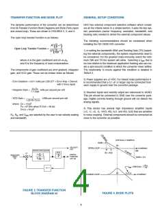
TRANSFER FUNCTION AND BODE PLOT
GENERAL SETUP CONDITIONS
The dynamic performance of the converter can be determined
from its Transfer Function Block Diagrams and Bode Plots (open
and closed loop)ꢀ These are shown in FIGURES ., 3, and 4ꢀ
DDC has external component selection software which consid-
ers all the criteria belowꢀ In a simple fashion, it asks the key sys-
tem parameters (carrier frequency, resolution, bandwidth, and
tracking rate) needed to derive the external component valuesꢀ
The open loop transfer function is as follows:
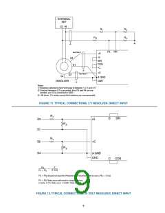
The following recommendations should be considered when
installing the RD-19.30 R/D converter:
S
A.
S.
+1
(B )
Open Loop Transfer Function =
S
1) In setting the bandwidth (BW) and Tracking Rate (TR) (select-
ing five external components), the system requirements need to
be consideredꢀ For the greatest noise immunity, select the mini-
mum BW and TR the system will allowꢀ Selecting a fBW that is
too low relative to the maximum application tracking rate can cre-
ate a spin-around condition in which the converter never settlesꢀ
The relationship to insure against this condition is detailed in
TABLE .ꢀ
+1
(10B )
where A is the gain coefficient and A.=A1A.
and B is the frequency of lead compensationꢀ
The components of gain coefficient are error gradient, integrator
gain, and VCO gainꢀ These can be broken down as follows:
.) Power supplies are 5 VDCꢀ For lowest noise performance it
is recommended that a 0ꢀ1 µF or larger cap be connected from
each supply to ground near the converter packageꢀ
- Error Gradient = 0ꢀ011 volts per LSB (CT + Error Amp + Demod
with . Vrms input)
Cs Fs
1ꢀ1 CBW
- Integrator Gain =
- VCO Gain =
volts per second per volt
LSBs per second per volt
3) Resolver inputs and velocity output are referenced to AGNDꢀ
This pin should be connected to GND near the converter pack-
ageꢀ Digital currents flowing through ground will not disturb the
analog signalsꢀ
1
1ꢀ.5 RV CVCO
where: Cs = 10 pF
Fs = 67 kHz when R CLK = 30 kΩ
4) This device has several high impedance amplifier inputs
(+C, -C, +S, -S, -VCO, VEL SJ1, and VEL SJ.) that are sensitive
to noise couplingꢀ External components should be connected as
close to the converter as possibleꢀ
CVCO = 50 pF
RV, RB, and CBW are selected by the user to set velocity scaling
and bandwidthꢀ
(CRITICALLY DAMPED)
GAIN = 4
.A
VELOCITY
OUT
ω (rad/sec)
10B
OPEN LOOP
B
A
-6 db/oct
ERROR PROCESSOR
VCO
(B = A/.)
CT
S
B
A
S
+ 1
1
A
S
DIGITAL
POSITION
OUT (φ)
+
.
RESOLVER
INPUT
(θ)
e
GAIN = 0ꢀ4
S
10B
+ 1
-
. A
fBW = BW (Hz) =
π
H = 1
.A
.
. A
ω (rad/sec)
CLOSED LOOP
FIGURE 3. TRANSFER FUNCTION
BLOCK DIAGRAM #2
FIGURE 4. BODE PLOTS
4

 ETC [ ETC ]