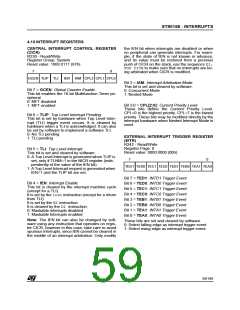
ST90158 - INTERRUPTS
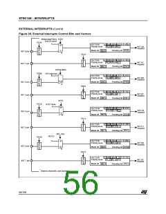
4.6 EXTERNAL INTERRUPTS
The standard ST9 core contains 8 external inter-
rupts sources grouped into four pairs.
Figure 25 shows an example of priority levels.
Figure 26 gives an overview of the External inter-
rupt control bits and vectors.
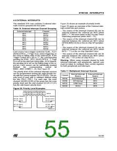
Table 10. External Interrupt Channel Grouping
– The source of the interrupt channel A0 can be
selected between the external pin INT0 (when
IA0S = “1”, the reset value) or the On-chip Timer/
Watchdog peripheral (when IA0S = “0”).
External Interrupt
Channel
INT7
INT6
INTD1
INTD0
INT5
INT4
INTC1
INTC0
– The source of the interrupt channel B0 can be
selected between the external pin INT2 (when
(SPEN,BMS)=(0,0)) or the on-chip SPI peripher-
al.
INT3
INT2
INTB1
INTB0
INT1
INT0
INTA1
INTA0
– The source of the interrupt channel C0 can be
selected between the external pin INT4 (when
INTS = “1”) or the on-chip Standard Timer.
Each source has a trigger control bit TEA0,..TED1
(R242,EITR.0,..,7 Page 0) to select triggering on
the rising or falling edge of the external pin. If the
Trigger control bit is set to “1”, the corresponding
pending bit IPA0,..,IPD1 (R243,EIPR.0,..,7 Page
0) is set on the input pin rising edge, if it is cleared,
the pending bit is set on the falling edge of the in-
put pin. Each source can be individually masked
– The source of the interrupt channel D0 can be
selected between the external pin INT6 (when
INT_SEL = “0”) or the on-chip RCCU.
Warning: When using channels shared by both
external interrupts and peripherals, special care
must be taken to configure their control registers
for both peripherals and interrupts.
through
the
corresponding
control
bit
IMA0,..,IMD1 (EIMR.7,..,0). See Figure 26.
Table 11. Multiplexed Interrupt Sources
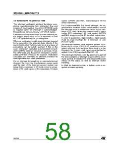
The priority level of the external interrupt sources
can be programmed among the eight priority lev-
els with the control register EIPLR (R245). The pri-
ority level of each pair is software defined using
the bits PRL2, PRL1. For each pair, the even
channel (A0,B0,C0,D0) of the group has the even
priority level and the odd channel (A1,B1,C1,D1)
has the odd (lower) priority level.
Internal Interrupt
Source
External Interrupt
Source
Channel
INTA0
INTB0
INTC0
INTD0
Timer/Watchdog
SPI Interrupt
STIM Timer
RCCU
INT0
INT2
INT4
INT6
Figure 25. Priority Level Examples
PL2D PL1D PL2C PL1C PL2B PL1B PL2A PL1A
1
0
0
0
1
0
0
1
EIPLR
SOURCE PRIORITY
SOURCE PRIORITY
INT.D0: 100=4
INT.A0: 010=2
INT.A1: 011=3
INT.D1:
101=5
INT.C0: 000=0
INT.C1: 001=1
INT.B0: 100=4
INT.B1: 101=5
VR000151
n
55/199
9

 ETC [ ETC ]