ST90158 - MULTIPROTOCOL SERIAL COMMUNICATIONS INTERFACE (SCI-M)
MULTIPROTOCOL SERIAL COMMUNICATIONS INTERFACE (Cont’d)
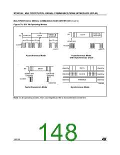
9.6.4.3 Serial Expansion Mode
the Clock Configuration Register. Whenever the
SCI is to receive data in synchronous mode, the
clock waveform must be supplied externally via
the RXCLK pin and be synchronous with the data.
For correct receiver operation, the XRX bit of the
Clock Configuration Register must be set.
This mode is used to communicate with an exter-
nal synchronous peripheral.
The transmitter only provides the clock waveform
during the period that data is being transmitted on
the CLKOUT pin (the Data Envelope). Data is
latched on the rising edge of this clock.
Two external signals, Request-To-Send and Data-
Carrier-Detect (RTS/DCD), can be enabled to syn-
chronise the data exchange between two serial
units. The RTS output becomes active just before
the first active edge of CLKOUT and indicates to
the target device that the MCU is about to send a
synchronous frame; it returns to its stand-by state
following the last active edge of CLKOUT (MSB
transmitted).
Whenever the SCI is to receive data in serial port
expansion mode, the clock must be supplied ex-
ternally, and be synchronous with the transmitted
data. The SCI latches the incoming data on the ris-
ing edge of the received clock, which is input on
the RXCLK pin.
9.6.4.4 Synchronous Mode
The DCD input can be considered as a gate that
filters RXCLK and informs the MCU that a trans-
mitting device is transmitting a data frame. Polarity
of RTS/DCD is individually programmable, as for
clocks and data.
This mode is used to access an external synchro-
nous peripheral, dummy start/stop bits are not in-
cluded in the data frame. Polarity, stand-by level
and active edges of I/O signals are fully and sepa-
rately programmable for both inputs and outputs.
The data word is programmable from 5 to 8 bits, as
for the other modes; parity, address/9th, stop bits
and break cannot be inserted into the transmitted
frame. Programming of the related bits of the SCI
control registers is irrelevant in Synchronous
Mode: all the corresponding interrupt requests
must, in any case, be masked in order to avoid in-
correct operation during data reception.
It's necessary to set the SMEN bit of the Synchro-
nous Input Control Register (SICR) to enable this
mode and all the related extra features (otherwise
disabled).
The transmitter will provide the clock waveform
only during the period when the data is being
transmitted via the CLKOUT pin, which can be en-
abled by setting both the XTCLK and OCLK bits of
147/199
9

 ETC [ ETC ]