ST6200C/ST6201C/ST6203C
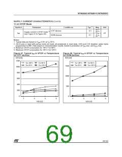
SUPPLY CURRENT CHARACTERISTICS (Cont’d)
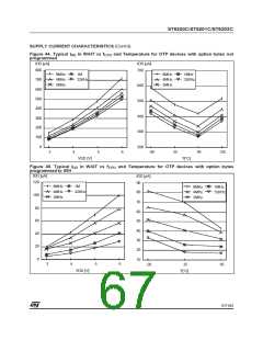
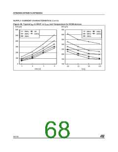
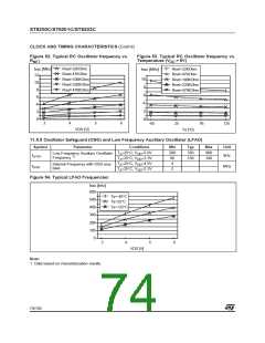
11.4.4 Supply and Clock System
The previous current consumption specified for
the ST6 functional operating modes over tempera-
ture range does not take into account the clock
source current consumption. To get the total de-
vice consumption, the two current values must be
added (except for STOP mode).
1)
2)
Symbol
Parameter
Conditions
=32kHz,
Typ
Max
Unit
f
f
f
f
f
OSC
OSC
OSC
OSC
OSC
=1MHz
=2MHz
=4MH
230
V
V
V
V
=5.0V
=3.3V
=5.0V
=3.3V
260
340
480
DD
DD
DD
DD
=8MHz
Supply current of RC oscillator
f
f
f
f
f
=32kHz,
=1MHz
=2MHz
=4MH
OSC
OSC
OSC
OSC
OSC
80
110
180
320
=8MHz
I
DD(CK)
f
f
f
f
f
=32kHz,
=1MHz
=2MHz
=4MH
900
280
240
140
40
OSC
OSC
OSC
OSC
OSC
µA
=8MHz
Supply current of resonator oscillator
f
f
f
f
f
=32kHz,
=1MHz
=2MHz
=4MH
120
70
50
20
10
OSC
OSC
OSC
OSC
OSC
=8MHz
3)
I
LFAO supply current
V
V
V
=5.0V
=5.0V
=5.0V
102
40
DD(LFAO)
DD
DD
DD
4)
I
OSG supply current
DD(OSG)
5)
I
LVD supply current
170
DD(LVD)
11.4.5 On-Chip Peripherals
Symbol
1)
Parameter
Conditions
Typ
Unit
V
V
V
V
=5.0V
170
100
80
DD
DD
DD
DD
6)
I
8-bit Timer supply current
f
=8MHz
DD(TIM)
OSC
=3.3V
=5.0V
=3.3V
µA
7)
I
ADC supply current when converting
f
OSC
=8MHz
DD(ADC)
50
Notes:
1. Typical data are based on T =25°C.
A
2. Data based on characterization results, not tested in production.
3. Data based on a differential I measurement between reset configuration (OSG and LFAO disabled) and LFAO run-
DD
ning (also includes the OSG stand alone consumption).
4. Data based on a differential I measurement between reset configuration with OSG disabled and OSG enabled.
DD
5. Data based on a differential I measurement between reset configuration with LVD disabled and LVD enabled.
DD
6. Data based on a differential I measurement between reset configuration (timer disabled) and timer running.
DD
7. Data based on a differential I measurement between reset configuration and continuous A/D conversions.
DD
70/104
1

 ETC [ ETC ]