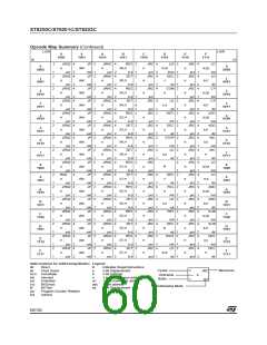
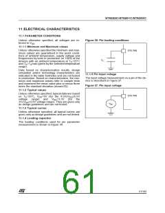
ST6200C/ST6201C/ST6203C
OPERATING CONDITIONS (Cont’d)
11.3.2 Operating Conditions with Low Voltage Detector (LVD)
Subject to general operating conditions for V , f
, and T .
A
DD OSC
Conditions
1)
Symbol
Parameter
Min
Typ
Max
Unit
Reset release threshold
V
3.9
4.1
4.3
IT+
(V rise)
DD
V
Reset generation threshold
V
V
3.6
50
3.8
4
IT-
(V fall)
DD
LVD voltage threshold hysteresis
V
-V
IT+ IT-
300
700
mV
mV/s
ns
hys
2)
Vt
V
rise time rate
DD
POR
3)
t
Filtered glitch delay on V
Not detected by the LVD
30
g(VDD)
DD
Notes:
1. LVD typical data are based on T =25°C. They are given only as design guidelines and are not tested.
A
2. The minimum V rise time rate is needed to insure a correct device power-on and LVD reset. Not tested in production.
DD
3. Data based on characterization results, not tested in production.
3)
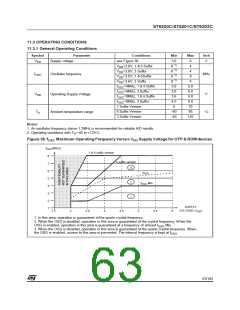
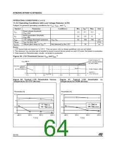
Figure 39. LVD Threshold Versus V and f
DD
OSC
FUNCTIONALITY
NOT GUARANTEED
IN THIS AREA
f
[MHz]
OSC
8
4
DEVICE UNDER
RESET
IN THIS AREA
FUNCTIONAL AREA
SUPPLY
VOLTAGE [V]
0
V
≥3.6
IT-
2.5
3
3.5
4
4.5
5
5.5
6
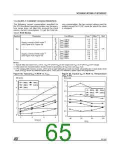
Figure 40. Typical LVD Thresholds Versus
Temperature for OTP devices
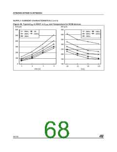
Figure 41. Typical LVD thresholds vs.
Temperature for ROM devices
Thresholds [V]
4.2
Thresholds [V]
4.2
4
4
V
Vdd up
V
IT+
Vdd up
IT+
V
IT-
Vdd down
V
3.8
3.6
Vdd down
3.8
3.6
IT-
-40°C
25°C
95°C
125°C
-40°C
25°C
95°C
125°C
T [°C]
T [°C]
64/104
1

 ETC [ ETC ]