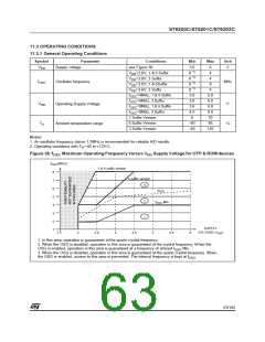
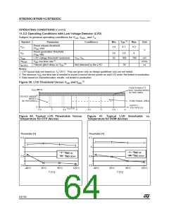
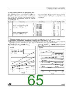
ST6200C/ST6201C/ST6203C
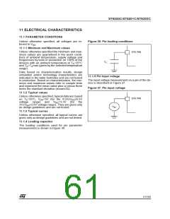
11.2 ABSOLUTE MAXIMUM RATINGS
Stresses above those listed as “absolute maxi-
mum ratings” may cause permanent damage to
the device. This is a stress rating only and func-
tional operation of the device under these condi-
tions is not implied. Exposure to maximum rating
conditions for extended periods may affect device
reliability.
11.2.1 Voltage Characteristics
Symbol
Ratings
Maximum value
Unit
V
- V
Supply voltage
7
DD
SS
1) & 2)
V
Input voltage on any pin
VSS-0.3 to VDD+0.3
3500
V
IN
V
Electro-static discharge voltage (Human Body Model)
ESD(HBM)
11.2.2 Current Characteristics
Symbol
Ratings
Maximum value
Unit
3)
3)
I
Total current into V
power lines (source)
DD
80
100
20
40
15
±5
VDD
I
Total current out of V ground lines (sink)
SS
VSS
Output current sunk by any standard I/O and control pin
Output current sunk by any high sink I/O pin
Output current source by any I/Os and control pin
Injected current on RESET pin
I
mA
IO
2) & 4)
I
INJ(PIN)
Injected current on any other pin
±5
11.2.3 Thermal Characteristics
Symbol
Ratings
Value
Unit
T
Storage temperature range
-60 to +150
°C
STG
Maximum junction temperature
(see THERMAL CHARACTERISTICS section)
T
J
Notes:
1. Directly connecting the RESET and I/O pins to V or V could damage the device if an unintentional internal reset
DD
SS
is generated or an unexpected change of the I/O configuration occurs (for example, due to a corrupted program coun-
ter). To guarantee safe operation, this connection has to be done through a pull-up or pull-down resistor (typical: 4.7kΩ
for RESET, 10kΩ for I/Os). Unused I/O pins must be tied in the same way to V or V according to their reset con-
DD
SS
figuration.
2. When the current limitation is not possible, the V absolute maximum rating must be respected, otherwise refer to
IN
I
specification. A positive injection is induced by V >V while a negative injection is induced by V <V
.
SS
INJ(PIN)
IN
DD
IN
3. Power (V ) and ground (V ) lines must always be connected to the external supply.
DD
SS
4. Negative injection disturbs the analog performance of the device. In particular, it induces leakage currents throughout
the device including the analog inputs. To avoid undesirable effects on the analog functions, care must be taken:
- Analog input pins must have a negative injection less than 1mA (assuming that the impedance of the analog voltage
is lower than the specified limits).
- Pure digital pins must have a negative injection less than 1mA. In addition, it is recommended to inject the current as
far as possible from the analog input pins.
62/104
1

 ETC [ ETC ]