ST6200C/ST6201C/ST6203C
11 ELECTRICAL CHARACTERISTICS
11.1 PARAMETER CONDITIONS
Unless otherwise specified, all voltages are re-
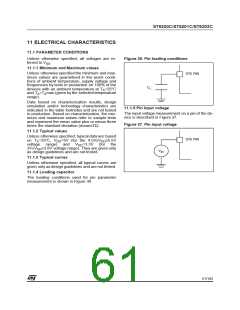
Figure 36. Pin loading conditions
ferred to V
.
SS
11.1.1 Minimum and Maximum values
Unless otherwise specified the minimum and max-
imum values are guaranteed in the worst condi-
tions of ambient temperature, supply voltage and
frequencies by tests in production on 100% of the
ST6 PIN
C
L
devices with an ambient temperature at T =25°C
A
and T =T max (given by the selected temperature
A
A
range).
Data based on characterization results, design
simulation and/or technology characteristics are
indicated in the table footnotes and are not tested
in production. Based on characterization, the min-
imum and maximum values refer to sample tests
and represent the mean value plus or minus three
times the standard deviation (mean±3Σ).
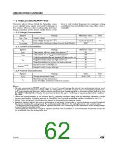
11.1.5 Pin input voltage
The input voltage measurement on a pin of the de-
vice is described in Figure 37.
Figure 37. Pin input voltage
11.1.2 Typical values
Unless otherwise specified, typical data are based
ST6 PIN
on T =25°C, V =5V (for the 4.5V≤V ≤5.5V
A
DD
DD
voltage range) and
V
DD
=3.3V (for the
3V≤V ≤3.6V voltage range). They are given only
DD
V
IN
as design guidelines and are not tested.
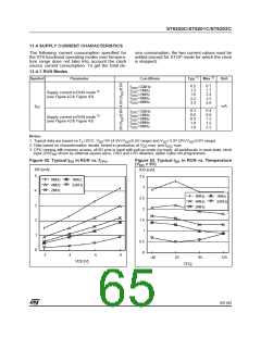
11.1.3 Typical curves
Unless otherwise specified, all typical curves are
given only as design guidelines and are not tested.
11.1.4 Loading capacitor
The loading conditions used for pin parameter
measurement is shown in Figure 36.
61/104
1

 ETC [ ETC ]