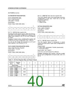
ST6200C/ST6201C/ST6203C
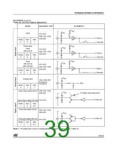
I/O PORTS (Cont’d)
8.2.5 Instructions NOT to be used to access
Port Data registers (SET, RES, INC and DEC)
2. Handling Unused Port Bits
On ports that have less than 8 external pins con-
nected:
DO NOT USE SINGLE-BIT INSTRUCTIONS
(SET, RES, INC and DEC) ON PORT DATA REG-
ISTERS IF ANY PIN OF THE PORT IS CONFIG-
URED IN INPUT MODE.
– Leave the unbonded pins in reset state and do
not change their configuration.
– Do not use instructions that act on a whole port
register (INC, DEC, or read operations). Unavail-
able bits must be masked by software (AND in-
struction). Thus, when a read operation
performed onan incomplete port is followed by a
comparison, use a mask.
These instructions make an implicit read and write
back of the entire register. In port input mode,
however, the data register reads from the input
pins directly, and not from the data register latch-
es. Since data register information in input mode is
used to set the characteristics of the input pin (in-
terrupt, pull-up, analog input), these may be unin-
tentionally reprogrammed depending on the state
of the input pins.
3. High Impedance Input
On any CMOS device, it is not recommended to
connect high impedance on input pins. The choice
of these impedance has to be done with respect to
the maximum leakage current defined in the da-
tasheet. The risk is to be close or out of specifica-
tion on the input levels applied to the device.
As a general rule, it is better to only use single bit
instructions on data registers when the whole (8-
bit) port is in output mode. In the case of inputs or
of mixed inputs and outputs, it is advisable to keep
a copy of the data register in RAM. Single bit in-
structions may then be used on the RAM copy, af-
ter which the whole copy register can be written to
the port data register:
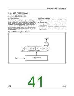
8.3 LOW POWER MODES
The WAIT and STOP instructions allow the
ST62xx to be used in situations where low power
consumption is needed. The lowest power con-
sumption is achieved by configuring I/Os in output
push-pull low mode.
SET bit, datacopy
LD a, datacopy
LD DRA, a
8.2.6 Recommendations
Mode
WAIT
STOP
Description
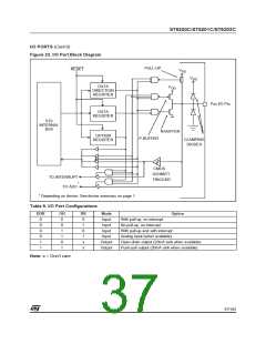
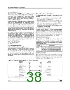
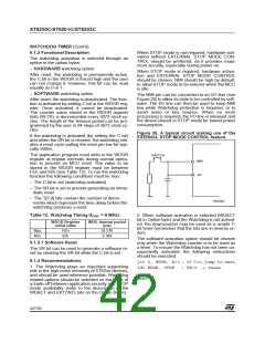
1. Safe I/O State Switching Sequence
No effect on I/O ports. External interrupts
cause the device to exit from WAIT mode.
Switching the I/O ports from one state to another
should be done in a sequence which ensures that
no unwanted side effects can occur. The recom-
mended safe transitions are illustrated in Figure 24
All other transitions are potentially risky and
should be avoided when changing the I/O operat-
ing mode.
No effect on I/O ports. External interrupts
cause the device to exit from STOP mode.
8.4 INTERRUPTS
The external interrupt event generates an interrupt
if the corresponding configuration is selected with
DDR, DR and OR registers (see Table 9) and the
GEN-bit in the IOR register is set.
Figure 24. Diagram showing Safe I/O State Transitions
Interrupt
pull-up
Input
Analog
010*
011
001
Input
pull-up (Reset
state)
000
Input
Output
Open Drain
Output
Open Drain
100
101
111
Output
110
Output
Push-pull
Push-pull
Note *. xxx = DDR, OR, DR Bits respectively
38/104
1

 ETC [ ETC ]