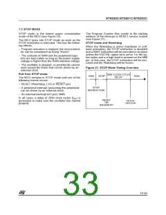
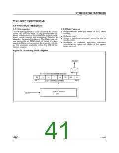
ST6200C/ST6201C/ST6203C
I/O PORTS (Cont’d)
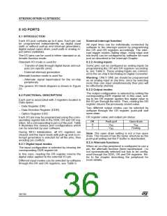
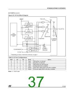
Figure 23. I/O Port Block Diagram
PULL-UP
RESET
V
DD
V
DD
DATA
DIRECTION
REGISTER
V
DD
Pxx I/O Pin
DATA
REGISTER
ST6
INTERNAL
BUS
N-BUFFER
OPTION
REGISTER
P-BUFFER
CLAMPING
DIODES
CMOS
SCHMITT
TRIGGER
TO INTERRUPT
*
TO ADC
* Depending on device. See device summary on page 1.
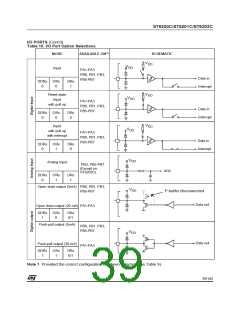
Table 9. I/O Port Configurations
DDR
OR
0
DR
0
Mode
Input
Option
0
0
0
0
1
1
With pull-up, no interrupt
No pull-up, no interrupt
0
1
Input
1
0
Input
With pull-up and with interrupt
Analog input (when available)
1
1
Input
0
x
Output
Output
Open-drain output (20mA sink when available)
Push-pull output (20mA sink when available)
1
x
Note: x = Don’t care
37/104
1

 ETC [ ETC ]