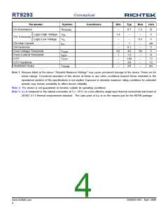
Conceptual
RT9293
Applications Information
V
LED Current Setting
IN
V
OUT
2.5V to 5.5V
L
D
10uH to 22uH
The loop of Boost structure will keep the FB pin voltage
equal to the reference voltage VREF. Therefore, when RREF
connects FB pin and GND, the current flows from VOUT
through LED and RREF to GND will be decided by the
current on RREF, which is equal to following equation.
C
1uF
OUT
C
IN
2.2uF
RT9293
LX
VOUT
EN
VIN
GND
WLEDs
Chip Enable
FB
VREF
R3
10k
ILED
=
RSET
R4
82k
R
SET
16
Dimming Control
V
Dimming
DC
0V to 2.8V
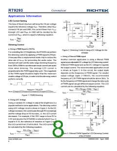
a. Using a PWM Signal to EN Pin
Figure 2. Dimming Control Using aDC Voltage for the
RT9293
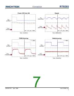
Forcontrolling the LED brightness, theRT9293can perform
the dimming control by applying a PWM signal to EN pin.
A low pass filter is implemented inside chip to reduce the
slew rate of IWLED for preventing the audio noise. The
internal soft start and the wide range dimming frequency
from 200 to 200kHz can eliminate inrush current and audio
noise when dimming. The average LED current is
proportional to the PWM signal duty cycle. The magnitude
of the PWM signal should be higher than the maximum
enable voltageof EN pin, in order to let the dimming control
perform correctly.
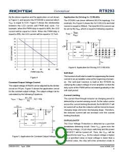
c. Using a Filtered PWM signal
Another common application is using a filtered PWM
signal as an adjustableDC voltage for LED dimming control.
A filtered PWM signal acts as theDC voltage to regulate
the output current. The recommended application circuit
is shown as Figure 3. In this circuit, the output ripple
depends on the frequency of PWM signal. For smaller
output voltage ripple (<100mV), the recommended
frequency of 2.8V PWM signal should be above 2kHz. To
fix the frequency of PWM signal and change the duty cycle
of PWM signal can get different output current. The LED
current can be calculated by the following equation.
EN
R3´ (V
´ Duty - V
)
I
= Duty of EN
PWM
REF
WLED,AVG
V
REF
-
I
R4 + R
WLED
DC
I
=
LED
R
SET
Figure 1. PWMDimming
V
IN
V
OUT
2.5V to 5.5V
L
b. Using aDC Voltage
D
10uH to 22uH
Using a variable DC voltage to adjust the brightness is a
popular method in some applications. The dimming control
using aDC voltage circuit is shown in Figure 2.As theDC
voltage increases, the current pass through R3 increasingly
and the voltage drop on R3 increase, i.e. the LED current
decreases. For example, if the VDC range is from 0V to
2.8V and assume the RT9293B is selected which VREF is
equal to 0.3V, the selection of resistors in Figure 2 sets
the LED current from 21mA to 0mA. The LED current can
be calculated by the following equation.
C
1uF
OUT
C
IN
2.2uF
RT9293
LX
VOUT
EN
VIN
GND
WLEDs
Chip Enable
FB
R3
10k
R4
3k
R
SET
16
C
DC
1uF
R
DC
82k
2.8V
0V
PWM Signal
R3´ (V - V
)
DC
REF
V
REF
-
R4
Figure 3. Filtered PWM Signal for LEDDimming Control
of the RT9293
I
=
LED
R
SET
www.richtek.com
8
DS9293-03C April 2008

 ETC [ ETC ]