Conceptual
RT9293
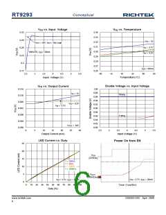
prevent abnormal function. As the die temperature >
160°C, the chip also will enter protection mode. The power
MOSFET will be turned off during protection mode to
prevent abnormal operation.
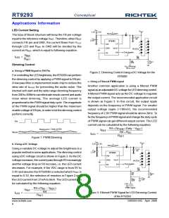
PD(MAX) = (125°C - 25°C) / (165°C/W) = 0.606W for
WDFN-8L 2x2 packages
PD(MAX) = (125°C - 25°C) / (255°C/W) = 0.392W for
TSOT-23-6 packages
The maximum power dissipation depends on operating
ambient temperature for fixed TJ(MAX) and thermal
resistance qJA. For RT9293 packages, the Figure 7 of
derating curves allows the designer to see the effect of
rising ambient temperature on the maximum power
allowed.
Inductor Selection
The recommended value of inductor for 10 WLEDs
applications is from 10uH to 22uH. Small size and better
efficiency are the major concerns for portable devices,
such as the RT9293 used for mobile phone. The inductor
should have low core loss at 1MHz and lowDCR for better
efficiency. The inductor saturation current rating should
be considered to cover the inductor peak current.
0.8
Single Layer PCB
0.7
Capacitor Selection
WDFN-8L 2x2
0.6
Input ceramic capacitor of 2.2uF and output ceramic
capacitor of 1uF are recommended for the RT9293
applications for driving 10 series WLEDs. For better
voltage filtering, ceramic capacitors with low ESR are
recommended. X5R and X7R types are suitable because
of their wider voltage and temperature ranges.
0.5
0.4
TSOT-23-6
0.3
0.2
0.1
0
Thermal Considerations
For continuous operation, do not exceed absolute
maximum operation junction temperature. The maximum
power dissipation depends on the thermal resistance of
IC package, PCB layout, the rate of surroundings airflow
and temperature difference between junction to ambient.
The maximum power dissipation can be calculated by
following formula :
0
25
50
75
100
125
(°C)
Ambient Temperature (°C)
Figure 7.Derating Curves for RT9293 Packages
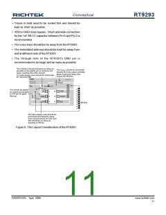
Layout Considerations
} A full GND plane without gap break.
PD(MAX) = ( TJ(MAX) - TA ) / qJA
} LX node copper area should be minimized for reducing
Where TJ(MAX) is the maximum operation junction
temperature 125°C, TA is the ambienttemperature and the
qJA is the junction to ambient thermal resistance.
EMI.
} The input capacitor CIN should be placed as closed as
possible to Pin 6.
For recommended operating conditions specification of
RT9293, where TJ(MAX) is the maximum junction
temperature of the die (125°C) and TA is the maximum
ambient temperature. The junction to ambient thermal
resistance qJA is layout dependent. For WDFN-8L 2x2
packages, the thermal resistance qJA is 165°C/W on the
standard JEDEC 51-3 single layer thermal test board. The
maximum power dissipation atTA = 25°C can be calculated
by following formula :
} The output capacitor COUT should be connected directly
from the Pin 5 to ground rather than across the LEDs.
} FB node copper area should be minimized and kept far
away from noise sources (Pin 1, Pin 5, Pin 6).
} The Inductor is far away receiver and microphone.
} RSET should be placed as close as possible to the
RT9293.
www.richtek.com
10
DS9293-03C April 2008

 ETC [ ETC ]