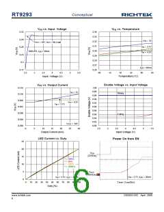
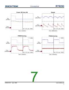
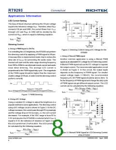
Conceptual
RT9293
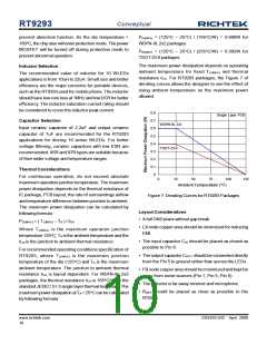
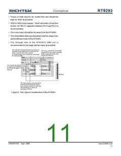
} Traces in bold need to be routed first and should be
kept as short as possible.
} VDD toGND noise bypass : Short and wide connection
for the 1uF MLCC capacitor between Pin 6 and Pin 2 is
recommended.
} The voice trace should be far away from the RT9293.
} The embedded antenna should be kept far away from
and at different side of the RT9293.
} The through hole of the RT9293's GND pin is
recommended to be large and as many as possible.
The inductor should be placed as close as
The C
should be connected
OUT
possible to the switch pin to minimize the
noise coupling into other circuits.
LX node copper area should be minimized
for reducing EMI.
directly from the output schottky
diode to ground rather than
across the WLEDs
GND
C
OUT
D
V
IN
L
C
should be placed
IN
LX
VIN
1
2
3
6
5
4
as closed as possible
to VIN pin for good
filtering.
C
IN
VOUT
EN
GND
SET
R
FB
WLEDs
FB node copper area should be
minimized and keep far away
from noise sources (LX pin) and
RS should be as close as
possible to FB pin.
Figure 8. The Layout Consideration of the RT9293
DS9293-03C April 2008
www.richtek.com
11

 ETC [ ETC ]