Conceptual
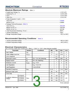
Absolute Maximum Ratings (Note 1)
RT9293
l Supply Input Voltage, VIN ---------------------------------------------------------------------------------------------- - 0.3V to 6V
l Switching Pin, LX -------------------------------------------------------------------------------------------------------- - 0.3V to 50V
l VOUT ----------------------------------------------------------------------------------------------------------------------- - 0.3V to 46V
l Other Pins----------------------------------------------------------------------------------------------------------------- - 0.3V to 6V
l PowerDissipation, PD @ TA = 25°C
TSOT-23-6 ----------------------------------------------------------------------------------------------------------------- 0.392W
WDFN- 8L 2x2 ------------------------------------------------------------------------------------------------------------ 0.606W
l Package Thermal Resistance (Note 3)
TSOT-23-6, qJA ----------------------------------------------------------------------------------------------------------- 255°C/W
WDFN- 8L 2x2, qJA------------------------------------------------------------------------------------------------------- 165°C/W
WDFN- 8L 2x2, qJC ------------------------------------------------------------------------------------------------------ 20°C/W
l Lead Temperature (Soldering, 10 sec.)------------------------------------------------------------------------------ 260°C
l JunctionTemperature --------------------------------------------------------------------------------------------------- 150°C
l StorageTemperature Range ------------------------------------------------------------------------------------------- - 65°C to 150°C
Recommended Operating Conditions (Note 2)
l Junction Temperature Range ------------------------------------------------------------------------------------------ - 40°C to 125°C
l AmbientTemperature Range ------------------------------------------------------------------------------------------ - 40°Cto 85°C
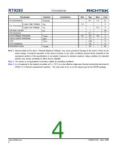
Electrical Characteristics
(VIN = 3.7V, CIN = 2.2uF, COUT = 0.47uF, IOUT = 20mA, L = 22uH, TA = 25°C, unless otherwise specified)
Parameter
Input Voltage
Symbol
Conditions
Min
2.5
2
Typ
--
Max
5.5
2.45
--
Unit
V
V
IN
Under Voltage Lock Out
UVLO Hystersis
V
UVLO
2.2
0.1
400
1
V
--
V
Quiescent Current
Supply Current
I
Q
FB = 1.5V, No Switching
FB = 0V, Switching
--
600
2
uA
mA
I
IN
--
Shutdown Current
Line Regulation
Load Regulation
Operation Frequency
Maximum Duty Cycle
Clock Rate
I
V
< 0.4V
--
--
1
1
4
--
uA
%
SHDN
EN
V
IN
= 3 to 4.3V
1mA to 20mA
--
1
--
%
f
0.75
90
0.1
94
1
1.25
--
MHz
%
OSC
92
--
200
114
kHz
RT9293A
RT9293B
RT9293C
104
Feedback Reference
Voltage
V
285
190
300
200
315
210
mV
REF
To be continued
DS9293-03C April 2008
www.richtek.com
3

 ETC [ ETC ]