Conceptual
RT9293
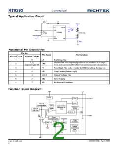
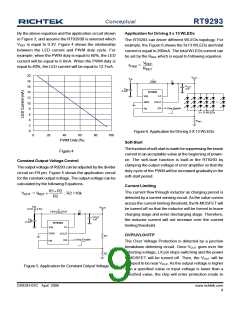
Typical Application Circuit
L
D
22uH
V
OUT
LX
VOUT
C
OUT
1uF
V
VIN
IN
C
IN
2.2uF
RT9293
10 WLEDs
Chip Enable
EN
GND
FB
R
SET
Functional Pin Description
Pin No.
Pin Name
Pin Function
□
RT9293 GJ6
□
RT9293 GQW
1
2
8
LX
Switching Pin.
1, 5,
Exposed pad (9)
Ground Pin. The exposed pad must be soldered to a large
PCB and connected to GND for maximum power dissipation.
GND
3
4
5
6
--
6
4
3
2
7
FB
Feed Back Pin, put a resistor to GND to setting the current.
Chip Enable (Active High).
Output Voltage Pin.
EN
VOUT
VIN
NC
Input Supply.
No Internal Condition.
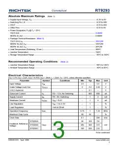
Function Block Diagram
LX
VIN
UVLO
OVP
OCP
VOUT
Internal
Compensation
OTP
Logic Control,
Minimum On
Time
Current-
Sense
PWM
-
Internal
Soft Start
+
+
Driver
EA
GM
GND
Slope
Compensation
Shutdown
20ms
PWM
Enable
Logic
Oscillator
LPF
Reference
Voltage
V
REF
Bias
Current
1uA
EN
FB
www.richtek.com
2
DS9293-03C April 2008

 ETC [ ETC ]