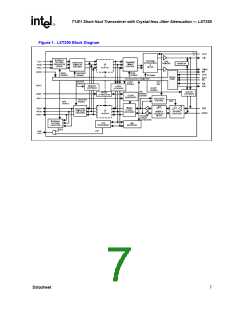
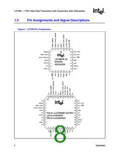
T1/E1 Short Haul Transceiver with Crystal-less Jitter Attenuation — LXT350
1.1
Mode Dependent Signals
As shown in Figure 2, the LXT350 has various signal pins that change function (and name)
according to the selected mode(s) of operation. These pins, associated signal names and operating
modes are summarized in Table 1 and Table 2. LXT350 signals are described in Table 3.
Table 1. LXT350 Clock and Data Pins by Mode1
Pin #
PLCC
External Data Modes
QRSS Modes
Unipolar Mode
QFP
Bipolar Mode
Unipolar Mode
Bipolar Mode
1
2
39
41
42
43
3
MCLK
TCLK
3
TPOS
TNEG
RNEG
RPOS
TDATA
INSBPV
BPV
INSLER
INSBPV
4
6
RNEG
RPOS
BPV
7
4
RDATA
RDATA
8
5
RCLK
TTIP
13
16
19
20
15
19
24
25
TRING
RTIP
RRING
1. Data pins change based on whether external data or internal QRSS mode is active. Clock pins remain the same in both
Hardware and Host modes.
Table 2. LXT350 Control Pins by Mode
Pin #
Hardware Modes
Host Modes
Pin #
PLCC
Hardware Modes
Host Modes
Unipolar/
QRSS
Unipolar/
Bipolar
Unipolar/
QRSS
Unipolar/
Bipolar
PLCC
QFP
QRSS
QFP
QRSS
Bipolar
Bipolar
5
9
2
7
MODE
TRSTE
JASEL
MODE
24
25
26
32
35
36
EC2
EC3
SDI
TRSTE
Low
SDO
CS
11
10
RLOOP
LOS/
LOS
LOS/
QPD
12
23
13
31
LOS
27
28
37
38
LLOOP
SCLK
CLKE
QPD
EC1
INT
TAOS
QRSS
Datasheet
9

 ETC [ ETC ]