Philips Semiconductors
Product specification
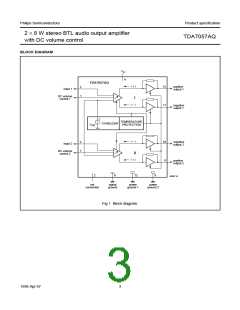
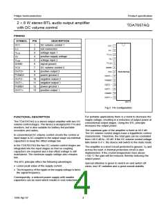
2 × 8 W stereo BTL audio output amplifier
with DC volume control
TDA7057AQ
CHARACTERISTICS
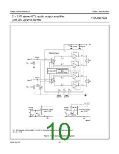
VP = 12 V;Tamb = 25 °C; fi = 1 kHz; RL = 16 Ω; unless otherwise specified (see Fig.13).
SYMBOL
VP
Iq(tot)
Maximum gain; V1,7 ≥ 1.4 V
PARAMETER
voltage supply
total quiescent current
CONDITIONS
MIN.
4.5
TYP.
MAX.
18.5
UNIT
−
V
VP = 12 V; RL = ∞; note 1
−
22
25
mA
Po
output power
THD = 10%; RL = 16 Ω
THD = 10%; RL = 8 Ω
3.0
−
3.5
5.3
8
−
−
−
W
W
W
THD=10%; RL = 8 Ω;
−
VP = 15 V
THD
Gv
total harmonic distortion
voltage gain
Po = 0.5 W
−
0.3
40.5
−
1
%
39.5
1
41.5
−
dB
V
Vi(rms)
Vo(n)
B
input signal handling (RMS value) Gv = 0 dB; THD < 1%
noise output voltage
bandwidth
fi = 500 kHz; note 2
at −1 dB
−
210
note 3
38
0
−
µV
dB
dB
mV
kΩ
dB
dB
dB
−
−
SVRR
VOS
Zi
supply voltage ripple rejection
DC output offset voltage
input impedance (pins 3 and 5)
channel separation
note 4
34
−
−
|V13 - V11| and |V10 - V8|
200
25
−
15
40
−
20
−
αcs
RS = 5 kΩ
Gv
channel unbalance
note 5
−
1
G1 = 0 dB; note 6
−
−
1
Mute position; V1 = V7 =0.4 V ±30 mV
Vo(mute) output voltage in mute position
DC volume control
Vi = 1.0 V; note 7
V1 = V7 = 0 V
−
35
45
µV
∆Gv
gain control range
volume control current
68
73.5
−
dB
lDC
−20
−25
−30
µA
Notes
1. With a load connected to the outputs the quiescent current will increase, the maximum value of this increase being
equal to the DC output offset voltage divided by RL.
2. The noise output voltage (RMS value) at fi = 500 kHz is measured with RS = 0 Ω and bandwidth = 5 kHz.
3. 20 Hz to 300 kHz (typical.
4. The ripple rejection is measured with RS = 0 Ω and f = 100 Hz to 10 kHz. The ripple voltage (Vripple = 200 mV RMS)
is applied to the positive supply rail.
5. The channel unbalance is measured with VDC1 = VDC2
6. The channel unbalance at G1 = 0 dB is measured with VDC1 = VDC2
7. The noise output voltage (RMS value) is measured with RS = 5 kΩ unweighted.
.
.
1998 Apr 07
6

 ETC [ ETC ]