Philips Semiconductors
Product specification
2 × 8 W stereo BTL audio output amplifier
with DC volume control
TDA7057AQ
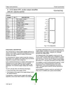
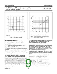
PINNING
SYMBOL
PIN
DESCRIPTION
DC volume control 1
handbook, halfpage
VC1
1
2
VC1
n.c.
1
2
n.c.
not connected
Vl (1)
3
voltage input 1
V
3
I (1)
VP
4
positive supply voltage
voltage input 2
V
P
4
Vl (2)
5
V
I (2)
5
SGND
VC2
6
signal ground
6
SGND
VC2
7
DC volume control 2
positive output 2
power ground 2
negative output 2
negative output 1
power ground 1
positive output 1
OUT2+
PGND2
OUT2−
OUT1−
PGND1
OUT1+
8
7
TDA7057AQ
9
OUT2
PGND2
OUT2
OUT1
8
10
11
12
13
9
10
11
PGND1 12
OUT1
13
MSA716
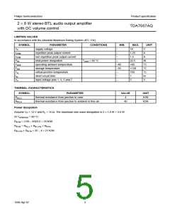
Fig.2 Pin configuration.
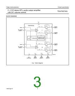
For portable applications there is a trend to decrease the
supply voltage, resulting in a reduction of output power at
conventional output stages. Using the BTL principle
increases the output power.
FUNCTIONAL DESCRIPTION
The TDA7057AQ is a stereo output amplifier with two DC
volume control stages. The device is designed for TVs and
monitors, but is also suitable for battery-fed portable
recorders and radios.
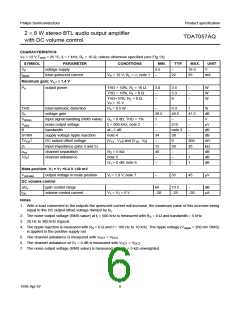
The maximum gain of the amplifier is fixed at 40.5 dB.
The DC volume control stages have a logarithmic control
characteristic. Therefore, the total gain can be controlled
from +40.5 dB to −33 dB. If the DC volume control voltage
falls below 0.4 V, the device will switch to the mute mode.
In conventional DC volume control circuits the control or
input stage is AC-coupled to the output stage via external
capacitors to keep the offset voltage low.
In the TDA7057AQ the two DC volume control stages are
integrated into the input stages so that no coupling
capacitors are required and a low offset voltage is still
maintained. The minimum supply voltage also remains
low.
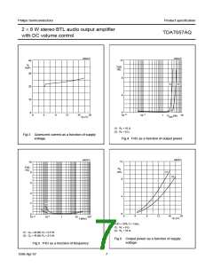
The amplifier is a short-circuit protected to ground, VP and
across the load. A thermal protection circuit is also
implemented. If the crystal temperature rises above
+150 °C the gain will be reduced, thereby reducing the
output power.
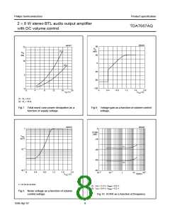
The BTL principle offers the following advantages:
Special attention is given to switch-on and switch-off
clicks, low HF radiation and a good overall stability.
• Lower peak value of the supply current
• The frequency of the ripple on the supply voltage is twice
the signal frequency.
Consequently, a reduced power supply with smaller
capacitors can be used which results in cost reductions.
1998 Apr 07
4

 ETC [ ETC ]