PRELIMINARY PRODUCT SPECIFICATION
nRF24L01 Single Chip 2.4 GHz Radio Transceiver
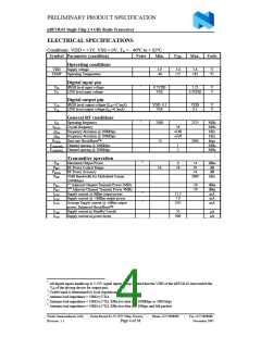
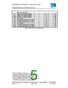
ELECTRICAL SPECIFICATIONS
Conditions: VDD = +3V, VSS = 0V, TA = - 40ºC to + 85ºC
Symbol Parameter (condition)
Notes
Min.
Typ.
Max.
Units
Operating conditions
VDD
TEMP
Supply voltage
1.9
-40
3.0
+27
3.6
+85
V
ºC
Operating Temperature
Digital input pin
HIGH level input voltage
LOW level input voltage
1
VIH
VIL
0.7VDD
VSS
5.25
0.3VDD
V
V
Digital output pin
HIGH level output voltage (IOH=-0.5mA)
LOW level output voltage (IOL=0.5mA)
VOH
VOL
VDD- 0.3
VSS
VDD
0.3
V
V
General RF conditions
Operating frequency
Crystal frequency
Frequency deviation @ 1000kbps
Frequency deviation @ 2000kbps
Data rate ShockBurst™
2
fOP
2400
>0
2525
2000
MHz
MHz
kHz
fXTAL
∆f1M
∆f2M
RGFSK
16
±160
±320
kHz
kbps
MHz
MHz
FCHANNEL Channel spacing @ 1000kbps
FCHANNEL Channel spacing @ 2000kbps
1
2
Transmitter operation
3
PRF
PRFC
PRFCR
PBW
Maximum Output Power
0
18
+4
20
±4
dBm
dB
dB
RF Power Control Range
RF Power Accuracy
20dB Bandwidth for Modulated Carrier
(2000kbps)
16
2000
kHz
PRF1
PRF2
IVDD
IVDD
IVDD
1st Adjacent Channel Transmit Power 2MHz
2nd Adjacent Channel Transmit Power 4MHz
Supply current @ 0dBm output power
Supply current @ -18dBm output power
Average Supply current @ -6dBm output
power, Enhanced ShockBurst™
Supply current in Standby-I mode
-20
-50
dBm
dBm
mA
mA
mA
4
5
11.3
7.0
0.05
IVDD
IVDD
32
900
µA
nA
Supply current in power down
1 All digital inputs handle up to 5.25V signal inputs. Keep in mind that the VDD of the nRF24L01 must match the
VIH of the driving device for output pins.
2 Usable band is determined by local regulations
3 Antenna load impedance = 100Ω+j175Ω
4 Antenna load impedance = 100Ω+j175Ω. Effective data rate 1000kbps or 2000 kbps
5 Antenna load impedance = 100Ω+j175Ω. Effective data rate 10kbps and full packets
Nordic Semiconductor ASA - Vestre Rosten 81, N-7075 Tiller, Norway
Revision: 1.1
-
Phone +4772898900
-
Fax +4772898989
November 2005
Page 4 of 38

 ETC [ ETC ]