PRELIMINARY PRODUCT SPECIFICATION
nRF24L01 Single Chip 2.4 GHz Radio Transceiver
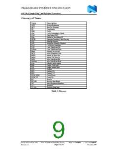
PIN FUNCTIONS
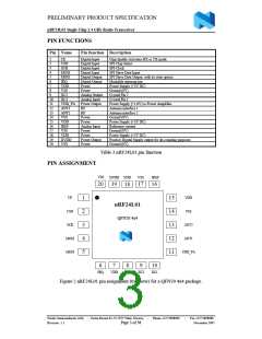
Pin Name
Pin function Description
1
2
3
4
5
6
7
8
CE
CSN
SCK
MOSI
MISO
IRQ
VDD
VSS
Digital Input
Digital Input
Digital Input
Digital Input
Digital Output
Digital Output
Power
Chip Enable Activates RX or TX mode
SPI Chip Select
SPI Clock
SPI Slave Data Input
SPI Slave Data Output, with tri-state option
Maskable interrupt pin
Power Supply (+3V DC)
Ground (0V)
Power
9
XC2
XC1
Analog Output
Analog Input
Power Output
RF
RF
Power
Power
Analog Input
Power
Power
Power Output
Power
Crystal Pin 2
Crystal Pin 1
Power Supply (+1.8V) to Power Amplifier
Antenna interface 1
Antenna interface 2
Ground (0V)
Power Supply (+3V DC)
Reference current
10
11
12
13
14
15
16
17
18
19
20
VDD_PA
ANT1
ANT2
VSS
VDD
IREF
VSS
VDD
DVDD
VSS
Ground (0V)
Power Supply (+3V DC)
Positive Digital Supply output for de-coupling purposes
Ground (0V)
Table 3 nRF24L01 pin function
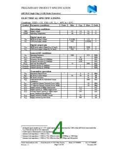
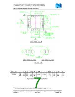
PIN ASSIGNMENT
VSS
DVDD
VSS
IREF
VDD
20 19
17 16
18
CE
VDD
VSS
1
15
14
13
12
11
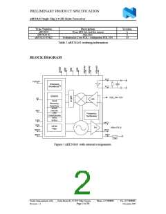
nRF24L01
CSN
2
QFN20 4x4
ANT2
ANT1
VDD_PA
SCK
3
MOSI
4
MISO
5
6
IRQ
7
VDD
8
VSS
9
XC2
10
XC1
Figure 2 nRF24L01 pin assignment (top view) for a QFN20 4x4 package.
Nordic Semiconductor ASA - Vestre Rosten 81, N-7075 Tiller, Norway
Revision: 1.1
-
Phone +4772898900
-
Fax +4772898989
November 2005
Page 3 of 38

 ETC [ ETC ]