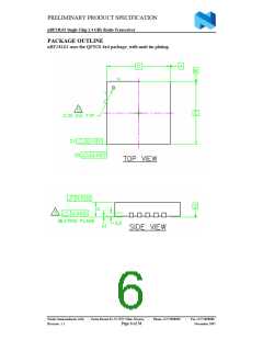
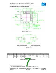
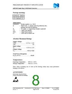
PRELIMINARY PRODUCT SPECIFICATION
nRF24L01 Single Chip 2.4 GHz Radio Transceiver
FUNCTIONAL DESCRIPTION
Modes of operation
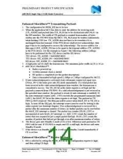
The nRF24L01 can be set in the following main modes depending on the level of the
following primary I/Os and configuration registers:
PWR_UP
register
PRIM_RX
register
CE
FIFO state
Mode
RX mode
TX mode
TX mode
1
1
1
1
0
0
1
1
ꢀ
-
Data in TX FIFO
1
0
Stays in TX mode until packet
transmission is finished
TX FIFO empty
No ongoing packet transmission
-
Standby-II
Standby-I
Power Down
1
1
0
0
-
-
1
0
-
Table 6 nRF24L01 main modes
An overview of the nRF24L01 I/O pins in different modes is given in Table 7.
Pin functions in the different modes of nRF24L01
Pin Name
CE
Direction
Input
TX Mode
High Pulse >10µs
RX Mode
Standby Modes Power Down
Low
High
-
CSN
SCK
Input
Input
SPI Chip Select, active low
SPI Clock
MOSI
MISO
Input
SPI Serial Input
SPI Serial Output
Tri-state
Output
Output
IRQ
Interrupt, active low
Table 7 Pin functions of the nRF24L01
Standby Modes
Standby-I mode is used to minimize average current consumption while maintaining
short start up times. In this mode, part of the crystal oscillator is active. In Standby-II
mode some clock buffers are active. Standby-II occurs when CE is held high on a
PTX device with empty TX FIFO. The configuration word content is maintained
during Standby modes. SPI interface may be activated. For start up time see Table 13.
Power Down Mode
In power down nRF24L01 is disabled with minimal current consumption. When
entering this mode the device is not active, but all registers values available from the
SPI interface are maintained during power down and the SPI interface may be
activated (CSN=0). For start up time see Table 13. The power down is controlled by
the PWR_UP bit in the CONFIG register.
Nordic Semiconductor ASA - Vestre Rosten 81, N-7075 Tiller, Norway
Revision: 1.1
-
Phone +4772898900
-
Fax +4772898989
November 2005
Page 10 of 38

 ETC [ ETC ]