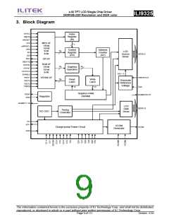
a-Si TFT LCD Single Chip Driver
240RGBx320 Resolution and 262K color
ILI9325
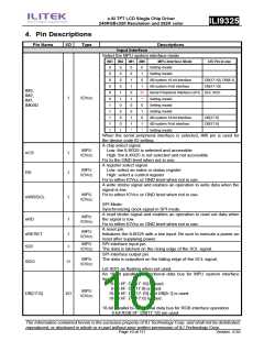
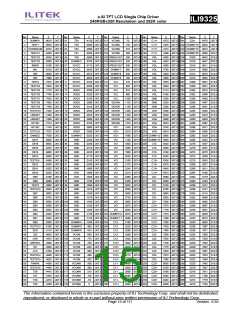
Pin Name
I/O
Type
Descriptions
16-bit RGB I/F: DB[17:13] and DB[11:1] are used.
18-bit RGB I/F: DB[17:0] are used.
Unused pins must be fixed to GND level.
Data ENEABLE signal for RGB interface operation.
Low: Select (access enabled)
MPU
IOVcc
High: Not select (access inhibited)
The EPL bit inverts the polarity of the ENABLE signal.
ENABLE
I
Fix to either IOVcc or GND level when not in use.
Dot clock signal for RGB interface operation.
MPU
IOVcc
DPL = “0”: Input data on the rising edge of DOTCLK
DPL = “1”: Input data on the falling edge of DOTCLK
Fix to the GND level when not in use
Frame synchronizing signal for RGB interface operation.
VSPL = “0”: Active low.
DOTCLK
VSYNC
I
I
MPU
IOVcc
VSPL = “1”: Active high.
Fix to the GND level when not in use.
Line synchronizing signal for RGB interface operation.
HSPL = “0”: Active low.
HSPL = “1”: Active high.
Fix to the GND level when not in use
MPU
IOVcc
HSYNC
FMARK
I
Output a frame head pulse signal.
MPU
IOVcc
O
The FMARK signal is used when writing RAM data in synchronization
with frame. Leave the pin open when not in use.
LCD Driving signals
Source output voltage signals applied to liquid crystal.
To change the shift direction of signal outputs, use the SS bit.
SS = “0”, the data in the RAM address “h00000” is output from S1.
SS = “1”, the data in the RAM address “h00000” is output from S720.
S1, S4, S7, … display red (R), S2, S5, S8, ... display green (G), and
S3, S6, S9, ... display blue (B) (SS = 0).
Gate line output signals.
VGH: the level selecting gate lines
VGL: the level not selecting gate lines
A supply voltage to the common electrode of TFT panel.
VCOM is AC voltage alternating signal between the VCOMH and
S720~S1
O
LCD
LCD
G320~G1
VCOM
O
O
TFT
common
electrode VCOML levels.
Stabilizing The high level of VCOM AC voltage. Connect to a stabilizing
capacitor capacitor.
Stabilizing The low level of VCOM AC voltage. Adjust the VCOML level with the
capacitor VDV bits. Connect to a stabilizing capacitor.
VCOMH
VCOML
O
O
GND or
external
resistor
Reference level for the grayscale voltage generating circuit. The VGS
level can be changed by connecting to an external resistor.
VGS
I
Charge-pump and Regulator Circuit
Power
supply
Power
supply
A supply voltage to the analog circuit. Connect to an external power
supply of 2.5 ~ 3.3V.
GND for the analog side: GND = 0V. In case of COG, connect to
GND on the FPC to prevent noise.
Vci
I
I
GND
An internal reference voltage for the step-up circuit1.
The amplitude between Vci and GND is determined by the VC[2:0]
bits.
Make sure to set the Vci1 voltage so that the DDVDH, VGH and VGL
voltages are set within the respective specification.
Stabilizing
capacitor
Vci1
O
O
DDVDH
Stabilizing Power supply for the source driver and Vcom drive.
The information contained herein is the exclusive property of ILI Technology Corp. and shall not be distributed,
reproduced, or disclosed in whole or in part without prior written permission of ILI Technology Corp.
Page 11 of 111
Version: 0.35

 ETC [ ETC ]