a-Si TFT LCD Single Chip Driver
240RGBx320 Resolution and 262K color
ILI9325
Write / Read rise / fall time
t
WRr/tWRf
ns
ns
-
10
5
-
-
-
-
-
-
-
-
25
Write ( RS to nCS, E/nWR )
Read ( RS to nCS, RW/nRD )
-
Setup time
tAS
-
Address hold time
5
tAH
tDSW
tH
ns
ns
ns
ns
ns
-
Write data set up time
Write data hold time
Read data delay time
Read data hold time
10
15
-
-
-
100
-
tDDR
tDHR
5
VIH
VIL
VIH
VIL
RS
nCS
tAS
tAH
PWLW, PWLR
PWHW, PWHR
VIH
VIH
VIL
VIH
nWR, nRD
VIL
tWRf
tWRr
tCYCW, tCYCR
tDSW
tH
VIH
VIL
VIH
VIL
Write Data
DB[17:0]
Valid Data
Valid Data
tDDR
tDHR
VOH
VOL
VOH
VOL
Read Data
DB[17:0]
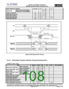
Figure 52 i80-System Bus Timing
14.4.2. Serial Data Transfer Interface Timing Characteristics
(IOVCC= 1.65 ~ 3.3V)
Item
Symbol
tSCYC
tSCYC
tSCH
Unit
µs
µs
ns
ns
ns
ns
ns
ns
ns
ns
ns
ns
Min.
100
200
40
Typ.
Max.
Test Condition
Write ( received )
Read ( transmitted )
Write ( received )
Read ( transmitted )
Write ( received )
Read ( transmitted )
-
-
-
-
-
-
-
-
-
-
-
-
-
Serial clock cycle time
-
Serial clock high – level
pulse width
-
100
40
tSCH
-
Serial clock low – level
pulse width
tSCL
-
100
-
tSCL
-
Serial clock rise / fall time
Chip select set up time
Chip select hold time
5
tSCr, tSCf
tCSU
10
-
50
tCH
-
Serial input data set up time
Serial input data hold time
Serial output data set up time
20
tSISU
tSIH
-
-
20
-
100
tSOD
The information contained herein is the exclusive property of ILI Technology Corp. and shall not be distributed,
reproduced, or disclosed in whole or in part without prior written permission of ILI Technology Corp.
Page 108 of 111
Version: 0.35

 ETC [ ETC ]