a-Si TFT LCD Single Chip Driver
240RGBx320 Resolution and 262K color
ILI9325
14.2. DC Characteristics
(VCC = VCI=2.40 ~ 3.0V, IOVCC = 1.65 ~ 3.30V, Ta= -40 ~ 85 °C)
Item
Symbol
Unit
Test Condition
Min.
0.8*IOVCC
-0.3
Typ.
Max.
IOVCC
Note
Input high voltage
Input low voltage
Output high voltage(1)
( DB0-17 Pins)
VIH
VIL
V
V
IOVCC= 1.8 ~ 3.3V
-
-
-
-
IOVCC= 1.8 ~ 3.3V
0.2*IOVCC
VOH1
V
IOH = -0.1 mA
0.8*IOVCC
-
-
-
Output low voltage
( DB0-17 Pins)
VOL1
ILI
IOP
V
IOVCC=1.65~3.3V
Vin = 0 ~ VCC
-
-
-
0.2*IOVCC
0.1
-
-
I/O leakage current
Current consumption
during normal operation
(VCC – GND )
µA
-0.1
VCC=2.8V , Ta=25°C , fOSC = 512KHz
( Line) GRAM data = 0000h
100
µA
µA
-
-
-
-
-
(VCC)
Current consumption
during standby mode
(VCC – GND )
IST
VCI=2.8V , Ta=25 °C
30
50
VCI=2.8V , VREG1OUT =4.8V
DDVDH=5.2V , Frame Rate: 70Hz,
line-inversion, Ta=25 °C, GRAM data =
0000h,
LCD Drive Power Supply
Current ( DDVDH-GND )
ILCD
mA
-
5.0
-
-
LCD Driving Voltage
( DDVDH-GND )
DDVDH
V
V
-
-
4.5
-10
-
-
6
-
-
Dispersion of the Average
Output Voltage
mV
10
14.3. Reset Timing Characteristics
Reset Timing Characteristics (IOVCC = 1.65 ~ 3.3 V)
Item
Symbol Unit
Min.
Typ.
Max.
Reset low-level width
Reset rise time
tRES
ms
µs
1
-
-
-
-
trRES
10
trRES
tRES
VIH
nRESET
VIL
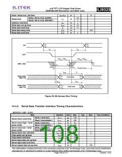
14.4. AC Characteristics
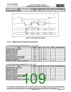
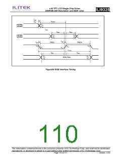
14.4.1. i80-System Interface Timing Characteristics
Normal Write Mode (IOVCC = 1.65~3.3V)
Item
Symbol
tCYCW
Unit
ns
Min. Typ.
Max. Test Condition
Write
Read
100
300
50
-
-
-
-
-
-
-
-
-
-
-
-
Bus cycle time
tCYCR
ns
-
Write low-level pulse width
Write high-level pulse width
Read low-level pulse width
Read high-level pulse width
PWLW
PWHW
PWLR
PWHR
ns
500
50
ns
-
-
-
150
150
ns
ns
The information contained herein is the exclusive property of ILI Technology Corp. and shall not be distributed,
reproduced, or disclosed in whole or in part without prior written permission of ILI Technology Corp.
Page 107 of 111
Version: 0.35

 ETC [ ETC ]