深圳市圣邦达电子有限公司
电话:086-0755-83723989 传真:086-0755-61351350
网 站 www.sbdsemi.cn EMAIL: yangbin7575@163.com
联系人:杨 生 13543266942 13642365547
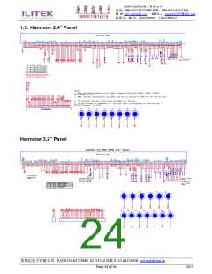
1.5. Hannstar 2.4” Panel
U1
HSD 2. 4" QVGA f or ILI9320
D1
C6
C7
0
C11 C1
C4
C5
2
C13
C1
C9
C8
1uF/6V
1uF/ 6V
All VCOM pins must be
1uF/6V
gether.
shorted to
IM3
0
IM0
0
Interface
16-bit i80-interface
VCI
1
0
1
1
8-bit i80-interface
0
1
18-bit i80-interface
9-bit i80-interface
When the RGB interface is used to transfer
the display data, the SPI interface is
necessary for the registers setting.
LED B/ L1
Note:
1. When the RGB interface is not used, please shorted the VSYNC, HSYNC, DOTCLK
and ENABLE to GND.
2. When the SPI interface is not used, the SDI is shorted to GND and let SDO as open.
3. The Schottky barrier diode shall be added for VGL pin.
4. If the voltage of interface is 1.8V, the IOVCC is connected to 1.8V and the
VCC/VCI connect to 2.8V.
TP1
TP2
TP3
TP4
TP5
TP6
TP7
VCL
TP8
CPUInterface
VCOM
VGH
VGL
DDVDH
VCI1
VREG1OUT
FMARK
J1
Hannstar 3.2” Panel
ILI9320 for HSD QVGA 3.2" Panel
U1
HSD 3.2" QVGA
f or ILI 9320
C 6
C 7
ALL the VCOM pins
must be shorted
together.
D1
On the default setting, the
internal resistor is used
OM pins
V
ALL the
must be sorted
together.
for the OSC and external
resistor can be removed.
ALL the VGL pins
must be shorted
together.
M3 M2 M1 M0
Interface Selection
i80-18bit interface
1
1
0
0
1
1
0
1
i80-9bit interface
i80-16bit interface
i80-8bit interface
SPI interface
0
0
0
1
1
1
0
0
1
ID
0
0
TP1
VGH
TP2
VGL
TP5
TP3
TP4
TP6
VCOMH
V C OML
VCOM
VREG1OUT
TP11
VCL
TP7
TP8
TP9
TP10
TP12
FMARK
TP13
GND
VCC
VCI
VCI
1
VD D
J1
J2
CON40
圣邦达电子有限公司 电话 0755-83723989 81753210 传真 0755-61351350 www.sbdsemi.cn
Page 24 of 34
V0.9

 ETC [ ETC ]