Data Sheet
June 1999
ORCA Series 2 FPGAs
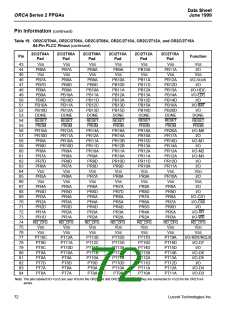
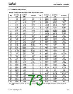
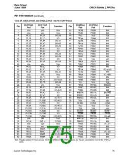
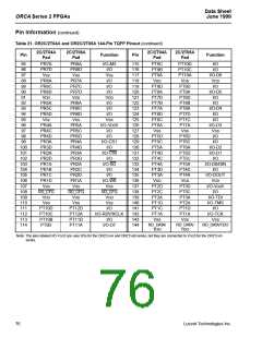
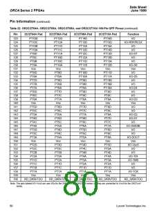
Pin Information (continued)
Table 21. OR2C/2T04A and OR2C/2T06A 144-Pin TQFP Pinout (continued)
2C/2T04A
Pad
2C/2T06A
Pad
2C/2T04A
Pad
2C/2T06A
Pad
Pin
Function
Pin
Function
85
86
87
88
89
90
91
92
93
94
95
96
97
98
99
100
101
102
103
104
105
106
107
108
109
110
111
112
113
114
PR7A
PR7D
VSS
PR6A
PR6C
PR6D
VDD
PR5A
PR5C
PR5D
VSS
PR4A
PR4C
PR4D
PR3A
PR3D
PR2A
PR2D
PR1A
PR1B
PR1C
PR1D
VSS
PR8A
PR8D
VSS
PR7A
PR7C
PR7D
VDD
PR6A
PR6C
PR6D
VSS
PR5A
PR5C
PR5D
PR4A
PR4D
PR3A
PR3D
PR2A
PR2C
PR2D
PR1A
VSS
I/O-M3
I/O
VSS
I/O
I/O
I/O
VDD
I/O
I/O
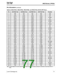
115
116
117
118
119
120
121
122
123
124
125
126
127
128
129
130
131
132
133
134
135
136
137
138
139
140
141
142
143
144
PT9C
PT9B
PT9A
VDD
PT8D
PT8A
PT7D
PT7B
PT7A
PT6D
PT6C
PT6A
VSS
PT5D
PT5C
PT5A
PT4D
PT4C
PT4A
PT3D
PT3A
VDD
PT2D
PT2C
PT2A
PT1D
PT1C
PT1A
VSS
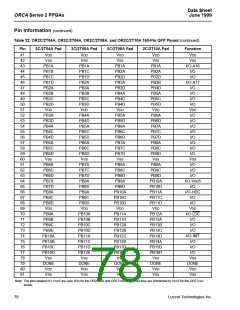
PT10D
PT10C
PT10A
VDD
PT9D
PT9A
PT8D
PT8B
PT8A
PT7D
PT7C
PT7A
VSS
PT6D
PT6C
PT6A
PT5D
PT5C
PT5A
PT4D
PT4A
VDD
PT3D
PT3C
PT3A
PT2A
PT1D
PT1A
VSS
I/O
I/O
I/O-D6
VDD
I/O
I/O-D5
I/O
I/O
I/O-D4
I/O
I/O
I/O-D3
VSS
I/O
VSS
I/O-VDD5
I/O
I/O
I/O-CS1
I/O
I/O-CS0
I/O
I/O-RD
I/O
I/O
I/O-WR
VSS
I/O
I/O
I/O-D2
I/O-D1
I/O
I/O-D0/DIN
I/O
I/O-DOUT
VDD
I/O-VDD5
I/O
I/O-TDI
I/O-TMS
I/O
RD_CFG
VDD
VSS
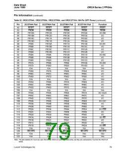
PT10D
PT10C
PT10B
PT9D
RD_CFG
VDD
VSS
PT12D
PT12A
PT11D
PT11A
RD_CFG
VDD
VSS
I/O
I/O-RDY/RCLK
I/O
I/O-TCK
VSS
RD_DATA/TDO
RD_DATA/
TDO
RD_DATA/
TDO
I/O-D7
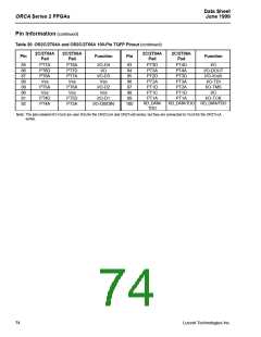
Note: The pins labeled I/O-VDD5 are user I/Os for the OR2CxxA and OR2TxxB series, but they are connected to VDD5 for the OR2TxxA
series.
76
Lucent Technologies Inc.

 ETC [ ETC ]