MITSUBISHI MICROCOMPUTERS
7470/7471 Group
SINGLE-CHIP 8-BIT CMOS MICROCOMPUTER
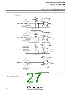
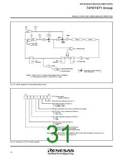
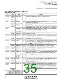
X
CIN
XCOUT
X
IN
XOUT
1/2
T34M
0
(Note 1)
1/8
Timer 3
Timer 4
1/2
CM
7
T34M
T34M
1
2
CM
6
7
CM
Internal clock φ
Q
S
S
S
R
Q
Q
Q
S
R
Reset
WIT
instruction
STP
instruction
R
R
STP instruction
Reset
Interrupt disable flag I
Interrupt request
Select gate : At reset, shaded
side is connected
Notes 1 : Refer to Timer 3 of [Figure 6 Block diagram of timer 1 through 4]
2 : 7470 group does not have XCIN input and XCOUT output.
Fig. 25 Block diagram of clock generating circuit
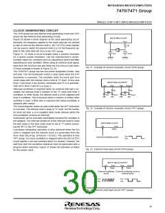
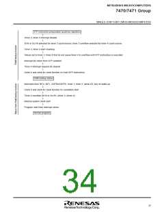
b7
b0
CPU mode register
(Address 00FB16)
These bits must always be set to “0”.
Stack page selection bit (Note 1)
0 : In page 0 area
1 : In page 1 area
Nothing is allocated (The value is undefined at reading)
S50, P51/XCIN, XCOUT selection bit (Note 2)
0 : P50, P51
1 : XCIN, XCOUT
XCOUT drive capacity selection bit (Note 2)
0 : Low
1 : High
Clock (XIN-XOUT) stop bit (Note 2)
0 : Oscillates
1 : Stops
Internal system clock selection bit (Note 2)
0 : XIN-XOUT selected (normal mode)
1 : XCIN-XCOUT selected (low-speed mode)
Notes 1 : In the M37470M2, M37470M4/E4, M37471M2, M37471M4/E4, set this bit to “0”.
2 : In the 7470 group, set this bit to “0”.
Fig. 26 Structure of CPU mode register
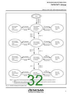
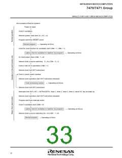
30

 ETC [ ETC ]