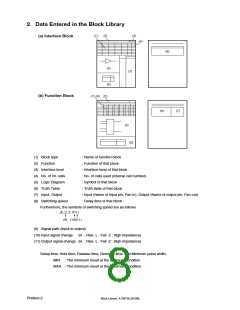
2. Data Entered in the Block Library
(1)
(2)
(3)
(a) Interface Block
(4)
(8)
(5)
(7)
(6)
(b) Function Block
(1),(4)
(2)
(8)
(7)
(5)
(6)
(1) Block type
: Name of function block
: Function of that block
(2) Function
(3) Interface level
(4) No. of int. cells
(5) Logic Diagram
(6) Truth Table
(7) Input, Output
(8) Switching speed
: Interface level of that block
: No. of cells used (internal cell number)
: Symbol of that block
: Truth table of that block
: Input (Name of input pin, Fan-in), Output (Name of output pin, Fan-out)
: Delay time of that block
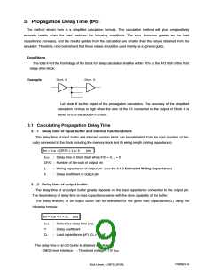
Furthermore, the symbols of switching speed are as follows
Y (H L)
A
(9) (10)(11)
(9) Signal path (input to output)
(10) Input signal change
(H : Rise L : Fall Z : High impedance)
(11) Output signal change (H : Rise L : Fall Z : High impedance)
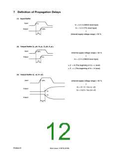
Setup time, Hold time, Release time, Removal time, and Minimum pulse width;
MIN : The minimum result at the minimum condition
MAX : The minimum result at the maximum condition
Preface-2
Block Library A13872EJ5V0BL

 ETC [ ETC ]