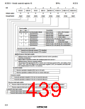
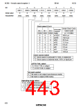
SCR1—Serial control register 1
H'A0
SCI1
Bit
7
SNC1
0
6
5
4
3
CKS3
0
2
CKS2
0
1
CKS1
0
0
SNC0 MRKON LTCH
CKS0
0
Initial value
Read/Write
0
0
0
R/W
R/W
R/W
R/W
R/W
R/W
R/W
R/W
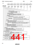
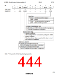
Clock select 2 to 0
Serial Clock Cycle
Clock Cycle
ø = 2.5 MHz
409.6 µs
102.4 µs
25.6 µs
Prescaler
Division
CKS2 CKS1 CKS0 Ratio
Bit 2 Bit 1 Bit 0
0
0
0
0
1
1
1
1
0
0
1
1
0
0
1
1
0
1
0
1
0
1
0
1
ø/1024
ø/256
ø/64
ø/32
ø/16
ø/8
12.8 µs
6.4 µs
3.2 µs
ø/4
1.6 µs
øW/4
122 µs
Clock source select
0
1
Clock source is prescaler S, SCK1 is output pin
Clock source is external clock, SCK1 is input pin
LATCH TAIL select
0
1
HOLD TAIL is output
LATCH TAIL is output
Tail mark control
0
1
Tail mark is not output (synchronous mode)
Tail mark is output (SSB mode)
Operating mode select
0
0
1
0
1
8-bit synchronous mode
16-bit synchronous mode
Continuous clock output mode
Reserved
1
428

 ETC [ ETC ]