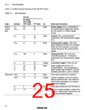
1.3.2
Pin Functions
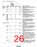
Table 1-2 outlines the pin functions of the H8/3887 Series.
Table 1-2 Pin Functions
Pin No.
FP-100B
TFP-100B
Type
Symbol
TFP-100G
FP-100A
I/O
Name and Functions
Power
source
pins
VCC
CVCC
38
32
41
35
Input
Power supply: All VCC connected to
the system power supply.pins should
be See section 14, Power Supply
Circuit.
VSS
11
33
14
36
Input
Input
Ground: All VSS pins should be
connected to the system power supply
(0 V).
AVCC
87
90
Analog power supply: This is the
power supply pin for the A/D converter.
When the A/D converter is not used,
connect this pin to the system power
supply.
AVSS
100
37
3
Input
Analog ground: This is the A/D
converter ground pin. It should be
connected to the system power supply
(0V).
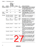
V0
40
Output
Input
LCD power supply: These are the
V1
V2
V3
36
35
34
39
38
37
power supply pins for the LCD
controller/driver. They incorporate a
power supply split-resistance, and are
normally used with V0 and V1 shorted.
Clock pins OSC1
OSC2
13
12
16
15
Input
These pins connect to a crystal or
Output
ceramic oscillator, or can be used to
input an external clock. See section 4,
Clock Pulse Generators, for a typical
connection diagram.
X1
X2
9
12
13
Input
These pins connect to a 32.768-kHz or
10
38.4-kHz crystal oscillator. Output See
section 4, Clock Pulse Genera–tors, for
a typical connection diagram.
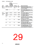
10

 ETC [ ETC ]