APEX 20K Programmable Logic Device Family Data Sheet
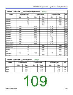
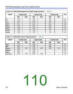
Table 114. Selectable I/O Standard Output Delays
Symbol
-1 Speed Grade
-2 Speed Grade
-3 Speed Grade
Unit
Min
Min
Max
Min
Max
Min
Max
LVCMOS
0.00
0.00
0.00
2.49
–0.03
0.75
1.39
1.11
1.35
1.00
–0.48
0.00
0.00
0.00
0.00
0.09
2.98
0.17
0.75
1.51
1.23
1.48
1.12
–0.48
0.00
0.00
0.00
0.00
0.10
3.03
0.16
0.76
1.50
1.23
1.47
1.12
–0.48
0.00
0.00
ns
ns
ns
ns
ns
ns
ns
ns
ns
ns
ns
ns
ns
LVTTL
2.5 V
1.8 V
PCI
GTL+
SSTL-3 Class I
SSTL-3 Class II
SSTL-2 Class I
SSTL-2 Class II
LVDS
CTT
AGP
To estimate device power consumption, use the interactive power
estimator on the Altera web site at http://www.altera.com.
Power
Consumption
The APEX 20K architecture supports several configuration schemes.
This section summarizes the device operating modes and available
device configuration schemes.
Configuration &
Operation
Operating Modes
The APEX architecture uses SRAM configuration elements that
require configuration data to be loaded each time the circuit powers
up. The process of physically loading the SRAM data into the device
is called configuration. During initialization, which occurs
immediately after configuration, the device resets registers, enables
I/ O pins, and begins to operate as a logic device. The I/ O pins are
tri-stated during power-up, and before and during configuration.
Together, the configuration and initialization processes are called
command mode; normal device operation is called user mode.
Before and during device configuration, all I/ O pins are pulled to
VCCIO by a built-in weak pull-up resistor.
112
Altera Corporation

 ETC [ ETC ]