IRQ Control Register 2. When programmed for pulse interrupt
mode, the associated interrupt pin will go low for 1 µS and return
high again. When programmed for LEVEL interrupt mode, the
interrupt will remain until the associated IRQ Status Register is
read, thus clearing the associated bits in each interrupt register.
Zero Wait Mode Operation: When Zero Wait Mode is enabled
by not grounding the ZERO WAIT pin, the host microprocessor
may read data from the DD-00429 shared memory resources
(DMT and Rx RAM) without using the READY or DTACK signals
to insert wait states into the microprocessor cycle. This is
accomplished by an additional “dummy read” of the desired
address. This dummy read causes the DD-00429 to fetch the
data from the source and place it in a latch. The data can then
be read from the latch (word-by-word or byte-by-byte) by read-
ing the same addresses.Thus for a 32-bit read in 8-bit mode, the
microprocessor would perform a total of five read operations.
The first read would be the dummy read; subsequent reads
would transfer the data.
Each of the individual interrupt registers can be masked by set-
ting their corresponding bit in IRQ Control Register 1. It should
be noted that the masking function only prevents the associated
IRQ pin from becoming active. When the mask bit is cleared, an
interrupt can occur in LEVEL IRQ mode if one or more interrupt
conditions occurred during the time when the mask was set. If
the user needs to ensure the interrupt will not occur upon clear-
ing the mask bit, the CPU should be programmed to read the
associated interrupt status register immediately prior to clearing
the IRQ mask bit.
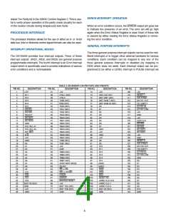
TABLE 4. DD-00429FP (160-PIN PQFP) ASIC PINOUTS
DESCRIPTION PIN NO. DESCRIPTION
81
PIN NO.
DESCRIPTION
PIN NO.
PIN NO.
DESCRIPTION
+5V
+5V
D11
1
41
42
43
44
45
46
47
48
49
50
51
52
53
54
55
56
57
58
59
60
61
62
63
64
65
66
67
68
69
70
71
72
73
74
75
76
77
78
79
80
+5V
+5V
121
122
123
124
125
126
127
128
129
130
131
132
133
134
135
136
137
138
139
140
141
142
143
144
145
146
147
148
149
150
151
152
153
154
155
156
157
158
159
160
2
XTAL1 (N/C)
XTAL2
82
83
OSC CLK OUT
RESET 1
CW STRB1
EN TX1 OUT
TX1 B IN
TX1 A IN
TX1 EMPTY
LD TX1 H1
LD TX1 LOW
+5V
3
D12
BIST T1A (N/C)
4
D13
TSB2 (N/C)
TSB3 (N/C)
TSA0 (N/C)
TSA1 (N/C)
TSA2 (N/C)
TSA3 (N/C)
TMA0 (N/C)
TMA1 (N/C)
TMA2 (N/C)
TMA3 (N/C)
TMA4 (N/C)
TMA5 (N/C)
TMA6 (N/C)
TMA7 (N/C)
TSB0 (N/C)
TSB1 (N/C)
+5V
84
BIST T1B (N/C)
5
D14
85
BIST DMT (N/C)
6
D15
86
BIST RAM7 (N/C)
7
EN RX1
EN RX0
SELECT
RX RDY1
RX RDY0
GND
87
BIST RAM24 (N/C)
8
88
D0
9
89
D1
10
11
12
13
14
15
16
17
18
19
20
21
22
23
24
25
26
27
28
29
30
31
32
33
34
35
36
37
38
39
40
90
D2
91
D3
GND
92
D4
+5V
POL SEL A1
POL SEL A0
INT/ MOT
8/16
93
D5
CHIP CLK
EN RX3
EN RX2
RX RDY 3
RX RDY 2
+5V
94
D6
95
D7
96
GND
+5V
97
+5V
TX0 A
TX0 B
TX1 A
TX1 B
GND
98
GND
99
+5V
GND
100
101
102
103
104
105
106
107
108
109
110
111
112
113
114
115
116
117
118
119
120
D8
RESET 0
CW STRB0
EN TX0 OUT
TX0B IN
TX0A IN
TX0 EMPTY
LOAD TX0 HI
LD TX0 LOW
GND
GND
D9
TMB0 (N/C)
TMB1 (N/C)
TMB2 (N/C)
TMB3 (N/C)
TMB4 (N/C)
TMB5 (N/C)
TMB6 (N/C)
TMB7 (N/C)
ZERO WAIT MODE
READY
D10
A0
D11
A1
D12
A2
D13
A3
D14
A4
D15
A5
(GND)
(GND)
IRQ3
A6
D0
A7
D1
A8
1RQ2
D2
A9
RD or DS
1RQ1
D3
A10
WR or RD/ WR
DTACK
RESET RC
ARINC CLK OUT
ARINC CLK 1
ARINC CLK 0
BIST R0 (N/C)
BIST R1 (N/C)
BIST R2 (N/C)
GND
D4
CS0
D5
CS1
ERROR
D6
CS2
MASTER RESET
+5V
D7
BIST R3 (N/C)
GND
D8
BIST TOA (N/C)
BIST TOB (N/C)
GND
D9
+5V
D10
GND
GND
5

 ETC [ ETC ]