ERROR INTERRUPT OPERATION
ciated Txn Parity bit in the ARINC Control Register 2.This is use-
ful to verify proper operation of the parity check circuitry for each
of the receive circuits during wraparound test mode.
When an error condition occurs, the ERROR output pin goes low
to indicate the presence of an error. The error pin will go high
again when the Error Status Register is clear. Each of these bits
is cleared by either reading the Error Status Register or remov-
ing the error condition.
PROCESSOR INTERFACE
The processor interface allows for the use of either an 8- or 16-bit
data bus. Intel or Motorola control signal formats can also be used.
GENERAL PURPOSE INTERRUPTS
INTERRUPT OPERATIONAL MODES
The three general purpose interrupt outputs can be used for mul-
tilevel interrupts or to trigger other external hardware for various
conditions. Each condition can be mapped to any one of the
three general purpose interrupts or disabled (by mapping to
IRQ0 which does not exist). Each interrupt output can be pro-
grammed to be either a LEVEL interrupt or PULSE interrupt via
The DD-00429 provides four interrupt outputs. Three of these
interrupt outputs (IRQ1, IRQ2, and IRQ3) are general purpose
programmable interrupts.The fourth interrupt is an Error interrupt
output which is specifically used to provide indications of various
error conditions and is nonmaskable.
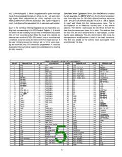
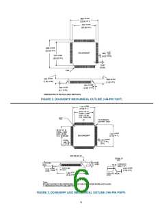
TABLE 3. DD-00429VP (144-PIN TQFP) ASIC PINOUTS
DESCRIPTION PIN NO. DESCRIPTION
73
PIN NO.
DESCRIPTION
PIN NO.
PIN NO.
DESCRIPTION
+5V
+5V
D11
1
37
38
39
40
41
42
43
44
45
46
47
48
49
50
51
52
53
54
55
56
57
58
59
60
61
62
63
64
65
66
67
68
69
70
71
72
+5V
+5V
109
110
111
112
113
114
115
116
117
118
119
120
121
122
123
124
125
126
127
128
129
130
131
132
133
134
135
136
137
138
139
140
141
142
143
144
2
XTAL1 (N/C)
XTAL2
74
75
OSC CLK OUT
RESET 1
CW STRB1
EN TX1 OUT
TX1 EMPTY
LD TX1 HI
LD TX1 LOW
+5V
3
D12
BIST DMT (N/C)
4
D13
TSB2 (N/C)
TSB3 (N/C)
TSA0 (N/C)
TSA1 (N/C)
TSA2 (N/C)
TSA3 (N/C)
TMA0 (N/C)
TMA1 (N/C)
TMA2 (N/C)
TMA3 (N/C)
TMA4 (N/C)
TMA5 (N/C)
TMA6 (N/C)
TMA7 (N/C)
TSB0 (N/C)
TSB1 (N/C)
+5V
76
BIST RAM 7 (N/C)
5
D14
77
BIST RAM 24 (N/C)
6
D15
78
D0
7
EN RX1
EN RX0
SELECT
RX RDY1
RX RDY0
GND
79
D1
8
80
D2
9
81
D3
GND
10
11
12
13
14
15
16
17
18
19
20
21
22
23
24
25
26
27
28
29
30
31
32
33
34
35
36
82
D4
+5V
83
D5
CHIP CLK
EN RX3
EN RX2
RX RDY3
RX RDY2
+5V
84
D6
POL SEL A1
POL SEL A0
INT/ MOT
8/16
85
D7
86
GND
87
+5V
88
GND
+5V
89
+5V
GND
GND
90
D8
RESET 0
CW STRB 0
EN TX0 OUT
TX0 EMPTY
LD TX0 HI
LD TX0 LOW
GND
A0
91
D9
A1
92
D10
A2
GND
93
D11
A3
TMB4 (N/C)
TMB5 (N/C)
TMB6 (N/C)
TMB7 (N/C)
ZERO WAIT MODE
READY
94
D12
A4
95
D13
A5
96
D14
A6
97
D15
D0
A7
98
(GND)
(GND)
IRQ3
D1
A8
99
D2
A9
RD or DS
100
101
102
103
104
105
106
107
108
D3
A10
WR or RD/WR
DTACK
IRQ2
D4
CS0
IRQ1
D5
CS1
ERROR
RESET RC
ARINC CLK OUT
ARINC CLK 1
ARINC CLK 0
BIST R2 (N/C)
GND
D6
CS2
MASTER RESET
+5V
D7
BIST R3 (N/C)
GND
D8
BIST TOA (N/C)
BIST TOB (N/C)
GND
D9
+5V
D10
GND
GND
4

 ETC [ ETC ]