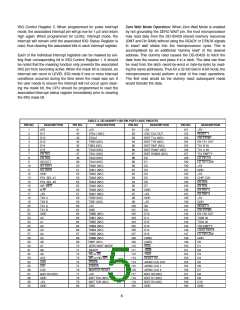
ARINC 429 RECEIVERS
the incoming ARINC 429 data contains a 00 in its S/D bit pair.
The DD-00429 supports four ARINC 429 inputs, designated
Receive channels 0 through 3 (Rx0, Rx1, Rx2 and Rx3). The
architecture of each of the four receiver circuits is identical and
each receives data independently. ARINC 429 data is directly
received into the DD-03282 ARINC 429 transceiver. Input pro-
tection, in accordance with the ARINC 429 specification, is pro-
vided along with voltage level translation from +5 V bipolar, non-
return-to-zero data to conventional, +5 V logic levels.
3) Receive Channel Number: Bits 12 and 13 of each DMT
entry are compared to the number of the channel which
received the ARINC 429 data.
A Data Match has occurred when all of the previous conditions
are satisfied; the data will then be stored in a RAM location
whose address equals the matching DMT entry minus 200 hex.
Bit 11 of each DMT entry, when set, will cause the incoming
ARINC 429 data to be stored in the corresponding receive chan-
nel FIFO (as well as the Rx RAM) when the data match condi-
tions are met.
Receive Data Rates can be programmed for channels 0 and 1
independently of channels 2 and 3 via bits 2 and 3 of ARINC
Control Register 2. The receiver circuitry will successfully
decode an incoming ARINC 429 data stream as long as the data
rate is within 5ꢀ of the nominal rate as determined by the Hi
Speed/Low Speed Bit and the associated ARINC Clock input
(ARINC CLK 0 or ARINC CLK 1). The two 1 MHz ARINC clock
inputs may be tied to the 1 MHz receive clock output or may be
connected to another clock source.The ARINC CLK input should
nominally be 10 times (for High-Speed Mode) or 80 times (for
Low-Speed mode) the desired ARINC Data Rate. ARINC CLK 0
is used by channels Rx0 and Rx1 while ARINC CLK 1 is used by
channels Rx2 and Rx3.
Bits 14 and 15 of each DMT entry provide the ability to cause
one of three general purpose interrupts upon a data match con-
dition. If set to “00” then no interrupt will occur upon a data match
condition (more information on interrupts is described later).
ARINC 429 TRANSMITTER(S)
The DD-00429 supports two ARINC 429 transmitters. Each of
these channels transmits data independently and are designat-
ed Tx0 and Tx1. The transmit output of the DD-00429 is a TTL
encoded digital data stream which can be connected directly to
DDC’s DD-03182 ARINC 429 line driver.
Filtering and Sorting Rx Data: The receiver circuitry converts
the serial data stream into a 32-bit-wide parallel data word. The
32-bit word is processed internally by a Data Match Processor
(DMP). It compares the incoming data to a table of data initial-
ized by the processor. This determines what incoming data is to
be saved, where it is going to be saved, and if any interrupts are
to be generated. The table of data is stored in a 128 word x 16
bit Data Match Table (DMT) RAM. When a match between the
received ARINC 429 data and the criteria stored in a DMT entry
is found, the received data, the storage address and modes, and
interrupt parameters are passed to the Data Store Processor
(DSP). The storage address in the Receive RAM is the address
of the first matching DMT entry minus 200 hex.
Transmit data rates can be programmed for Channels 0 and 1
independently. The transmit data rate is determined by the High-
Speed/Low-Speed Bit for each of the Tx channels in ARINC
Control Register 2 and the associated ARINC Clock input
(ARINC CLK 0 or ARINC CLK 1). The two, 1 MHz ARINC clock
inputs may be tied to the 1 MHz clock output or they may be con-
nected to another clock source to achieve transmit data rates
other than 100 kHz or 12.5 kHz. The transmit clock input should
be 10 times (for High-Speed Mode) or 80 times (for Low-Speed
mode) the desired ARINC transmit data rate.
There are three requirements that must be met in order to match
incoming ARINC 429 data to each DMT entry:
Transmit FIFOs: Each transmitter channel is provided with an
output FIFO which is 32 words deep by 32 bits wide. When writ-
ing data to the Tx FIFO, the associated Disable Txn bit in ARINC
Control Register 1 can be set to a logic zero until the FIFO is
loaded with the desired data. Upon setting the Disable Txn low
the transmit channel will send the 32-bit message words with
appropriate interword gaps on the ARINC 429 output. A status
bit indicating that the FIFO is empty is supplied for each trans-
mitter in the ARINC Status Register.
1) System Address Label: Bits 0-7 of the DMT are compared
to the System Address Label (SAL) of the incoming ARINC
429 data word. If the DMT SAL entry is zero then the SAL of
the incoming data word is ignored (or considered a match).
2) Source/Destination Bits: Bits 8 and 9 of each DMT entry
are compared to the Source/Destination (S/D) bits of the
incoming ARINC 429 data word. If these bits match, or if Bit
10 of the DMT entry is set to a 1, then the S/D bit comparison
is considered a match. It is also possible, through DMP
Control Register 1, to enable “All Call Mode” as defined in the
ARINC 429 specification. When enabled for a particular
receive channel, the S/D bits will be considered a match when
Wraparound testing can be performed from Tx0 to Rx0 and Rx1
and from Tx1 to Rx2 and Rx3. The data received on Rx1 and
Rx3 in wraparound test mode is inverted. Wraparound testing is
enabled by setting the appropriate bits in ARINC Control
Register 1. The parity of the transmitted word can be altered to
even parity (instead of the usual odd parity) by setting the asso-
3

 ETC [ ETC ]