Si3210/Si3211/Si3212
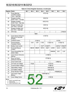
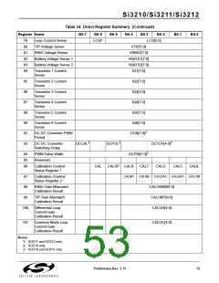
Table 34. Direct Register Summary (Continued)
Register Name
Bit 7
Bit 6
Bit 5
Bit 4
Bit 3
Bit 2
Bit 1
Bit 0
79
80
81
82
83
84
Loop Current Sense
LCSP
LCS[5:0]
TIP Voltage Sense
VTIP[7:0]
RING Voltage Sense
Battery Voltage Sense 1
Battery Voltage Sense 2
VRING[7:0]
VBATS1[7:0]
VBATS2[7:0]
IQ1[7:0]
Transistor 1 Current
Sense
85
86
87
88
89
92
93
Transistor 2 Current
Sense
IQ2[7:0]
IQ3[7:0]
IQ4[7:0]
IQ5[7:0]
IQ6[7:0]
Transistor 3 Current
Sense
Transistor 4 Current
Sense
Transistor 5 Current
Sense
Transistor 6 Current
Sense
3
DC-DC Converter PWM
Period
DCN[7:0]
2
2
2
DC-DC Converter
Switching Delay
DCCAL
DCPOL
DCTOF[4:0]
CALD
2
94
95
96
PWM Pulse Width
Reserved
DCPW[7:0]
Calibration Control/
Status Register 1
CAL
CALSP CALR
CALT
CALC
CALIL
CALM1 CALM2 CALDAC CALADC CALCM
97
98
Calibration Control/
Status Register 2
RING Gain Mismatch
Calibration Result
CALGMR[R4:0]
CALGMT[4:0]
CALGD[4:0]
99
TIP Gain Mismatch
Calibration Result
100
Differential Loop
Current Gain
Calibration Result
101
Common Mode Loop
Current Gain
CALGC[4:0]
Calibration Result
Notes:
1. Si3211 and Si3212 only.
2. Si3210 only.
3. Si3210 and Si3211 only.
Preliminary Rev. 1.11
53

 ETC [ ETC ]