PCT1789W DATA SHEET
PRELIMINARY
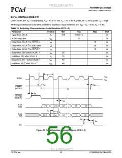
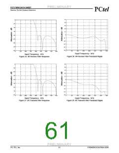
SWITCHING CHARACTERISTICS
!!
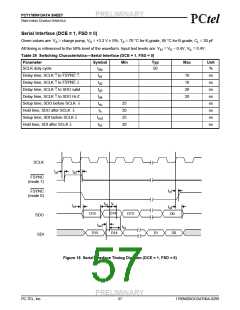
Serial Interface (DCE = 1, FSD = 0)
Given values are: VA = charge pump, VD = +3.3 V ± 5%; TA = 70 °C for K-grade, 85 °C for B-grade; CL = 20 pF.
All timing is referenced to the 50% level of the waveform. Input test levels are: VIH = VD – 0.4V, VIL = 0.4V.
Table 26 Switching Characteristics—Serial Interface (DCE = 1, FSD = 0)
Parameter
Symbol
Min
Typ
Max
Unit
SCLK duty cycle
tdty
50
%
Delay time, SCLK • to FSYNC •
Delay time, SCLK • to FSYNC ¯
Delay time, SCLK • to SDO valid
Delay time, SCLK • to SDO Hi-Z
Setup time, SDO before SCLK ¯
Hold time, SDO after SCLK ¯
Setup time, SDI before SCLK ¯
Hold time, SDI after SCLK ¯
td1
td2
td3
td4
tsu
th
10
10
20
20
ns
ns
ns
ns
ns
ns
ns
ns
25
20
25
20
tsu2
th2
SCLK
td1
td2
FSYNC
(mode 1)
td1
FSYNC
(mode 0)
tsu th
td3
td4
D0
D14
D15
D13
SDO
SDI
tsu2
D15
th2
D14
D1
D0
Figure 18 Serial Interface Timing Diagram (DCE = 1, FSD = 0)
PRELIMINARY
PC-TEL, Inc.
57
1789W0DOCDAT06A-0299

 ETC [ ETC ]