PCT1789W DATA SHEET
PRELIMINARY
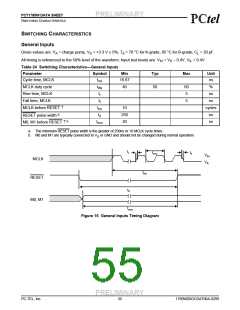
SWITCHING CHARACTERISTICS
!!
SWITCHING CHARACTERISTICS
General Inputs
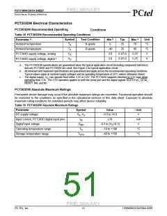
Given values are: VA = charge pump, VD = +3.3 V ± 5%; TA = 70 °C for K-grade, 85 °C for B-grade; CL = 20 pF.
All timing is referenced to the 50% level of the waveform. Input test levels are: VIH = VD – 0.4V, VIL = 0.4V.
Table 24 Switching Characteristics—General Inputs
Parameter
Symbol
Min
Typ
Max
Unit
Cycle time, MCLK
tmc
16.67
ns
MCLK duty cycle
tdty
tr
40
50
60
5
%
ns
Rise time, MCLK
Fall time, MCLK
tf
5
ns
MCLK before RESET •
RESET pulse width a
M0, M1 before RESET •
tmr
trl
10
250
20
cycles
ns
b
tmxr
ns
a. The minimum RESET pulse width is the greater of 250ns or 10 MCLK cycle times.
b. M0 and M1 are typically connected to VD or GND and should not be changed during normal operation.
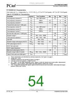
tr
tmc
tf
VIH
VIL
MCLK
tmr
RESET
trl
M0, M1
tmxr
Figure 16 General Inputs Timing Diagram
PRELIMINARY
PC-TEL, Inc.
55
1789W0DOCDAT06A-0299

 ETC [ ETC ]